Download presentation
Presentation is loading. Please wait.

1
Feb. 17, 2011 Midterm overview Real life examples of built chips
Clock Skew Arithmetic Data Centers Power reduction techniques Dynamic Voltage / Frequency Scaling Clock Throttling Power Gating Others? Project – 4b adder with Razor recovery

3
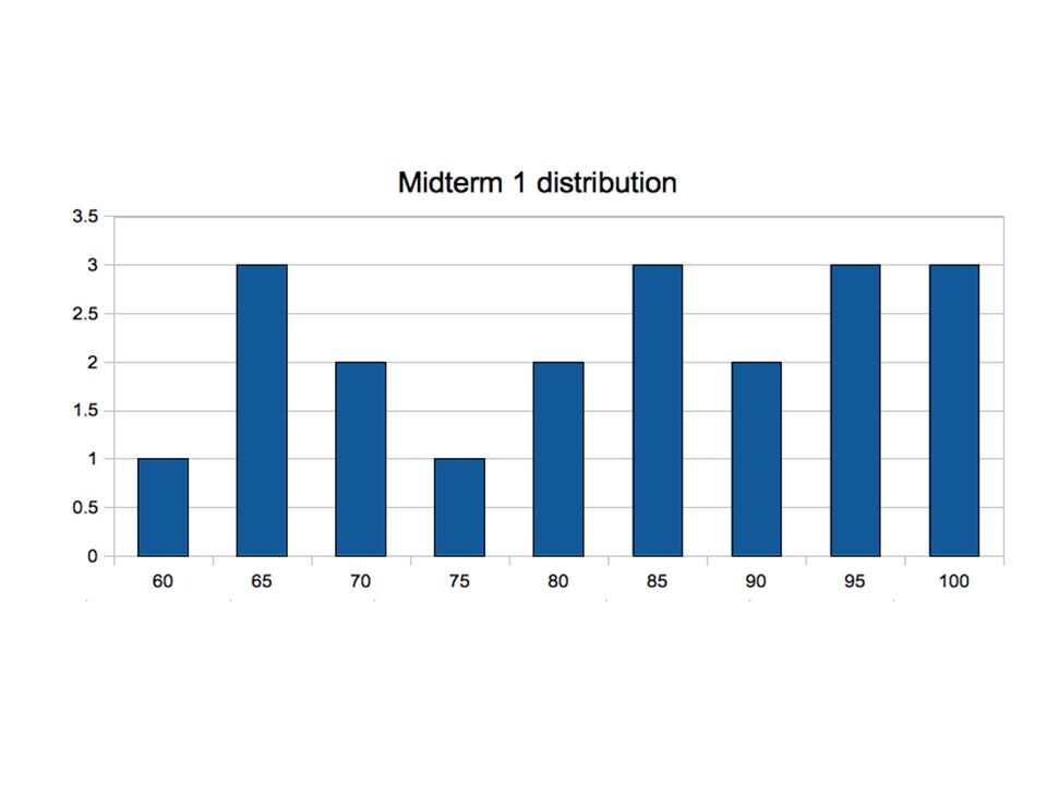
Go Over Problems 1c 2a; 2b 3c

4
Crossbar Design

6
Mirror Adder Stick Diagram

7
The Mirror Adder The NMOS and PMOS chains are completely symmetrical. A maximum of two series transistors can be observed in the carry- generation circuitry. When laying out the cell, the most critical issue is the minimization of the capacitance at node Co. The reduction of the diffusion capacitances is particularly important. The capacitance at node Co is composed of four diffusion capacitances, two internal gate capacitances, and six gate capacitances in the connecting adder cell . The transistors connected to Ci are placed closest to the output. Only the transistors in the carry stage have to be optimized for optimal speed. All transistors in the sum stage can be minimal size.

8
Transmission Gate Full Adder

9
Manchester Carry Chain

10
Manchester Carry Chain

11
Carry-Bypass Adder Also called Carry-Skip

12
Carry-Bypass Adder (cont.)
")
13
Carry Ripple versus Carry Bypass

14
Carry-Select Adder

15
Carry Select Adder: Critical Path

16
Linear Carry Select

17
Square Root Carry Select

18
Adder Delays - Comparison

19
LookAhead - Basic Idea

20
Look-Ahead: Topology Expanding Lookahead equations: All the way:

21
Carry Lookahead Trees Can continue building the tree hierarchically.

23
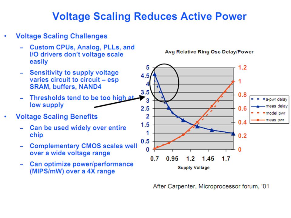
Power Reduction Techniques
Stop the clock Dynamic power reduction Power gating Reduce the leakage How fast can you turn something on/off? Nothing to do sleep How can you save power while in operation? Near-threshold design

24
Power Gating

27
Kevin Nowka, IBM

33
Gate Leakage

35
Digital Parallelization
Y[n] = X[n] + X[n-1] Input 5GS/s) Analog Signal X[n-1] X[n] Input 5GS/s) Or 100MHz) clk clk x Y[n] + Clk = 5GHz ANALOG DIGITAL
 Analog Signal. X[n-1] X[n] Input. 5GS/s) Or. 100MHz) clk. clk. x. Y[n] + Clk = 5GHz. ANALOG. DIGITAL.")
36
DSP Parallelization Y[n] = X[n] + X[n-1] Y[n-1] = X[n-1] + X[n-2]
Input 5GS/s) Y[n] + clk clk x Y[n-1] + clk X[n-1] x clkb clk CLK = 5GHz CLK = 2.5GHz
![DSP Parallelization Y[n] = X[n] + X[n-1] Y[n-1] = X[n-1] + X[n-2]](http://slideplayer.com/slide/1653664/7/images/36/DSP+Parallelization+Y%5Bn%5D+%3D+X%5Bn%5D+%2B+%EF%81%A1X%5Bn-1%5D+Y%5Bn-1%5D+%3D+X%5Bn-1%5D+%2B+%EF%81%A1X%5Bn-2%5D.jpg "Input. 5GS/s) Y[n] + clk. clk. x. Y[n-1] + clk. X[n-1] x. clkb. clk. CLK = 5GHz. CLK = 2.5GHz.")
37
DSP Parallelization Clock speed reduced by ½ Intuition?
Can parallelize further Increase number of MACs(multiply/accumulates) by 2 Intuition? Area goes up by 2 Power decreases (clock rate down by 2, computations up by 2, but easier timing constraints) What about clock power? Save a little power, but double the area?
 by 2. Intuition Area goes up by 2. Power decreases (clock rate down by 2, computations up by 2, but easier timing constraints) What about clock power Save a little power, but double the area")
38
Razor: A Low-Power Pipeline Based on Circuit-Level Timing Speculation

45
Project Description Minimal: 4b Adder, Implemented with Razor
Simulations into near-threshold domain Grad. Student: requires more advanced design Analog: Opamps built using inverters Digital: Adiabatic Near-Threshold Power Gating: add power gating to your design Undergrad: extra credit if do any of the above

46
Problem 1: On-Chip Wires Consume Energy
On-chip wire power does not scale Dominated by interconnect capacitance (CVDD2) VDD Eb 1V 150fJ/mm ON-CHIP (Status Quo): fJ/bit/mm On-chip wires start to dominate power consumption, as computational logic energy is minimized when operating in near-threshold. Here is a graph for a recent DOE exascale study, showing that in the next 8 years, the energy to perform a double-precision FLOP will improve by 5x, but on-chip wires will not. For example, 1mm and 5mm on-chip links will not have changed, because energy is proportional to capacitance, and fringe capacitance will not improve with technology scaling. Note that from our initial work with near-threshold computation, the amount of energy it takes to perform a 16b multiply/Accumulate is 200fJ for Vdd=0.4V. The amount Of energy to move that 16b parallel bus 300um distance will cost 250fJ – or more energy than it takes to perform computation. Hence, low-Vdd operation accentuates to the problem of energy-consumption within on-chip wires. We will need to propose another 5-10x improvement in energy-efficiency for on-chip wires in order to close this gap when logic operates in near-threshold regime. OUR GOAL: < 5fJ/bit/mm NOTE: Sub/Near-Threshold doesn’t help this problem! [DOE, Exascale Workshop]
 VDD. Eb. 1V. 150fJ/mm. ON-CHIP (Status Quo): fJ/bit/mm. On-chip wires start to dominate power consumption, as computational logic energy is minimized when operating in near-threshold. Here is a graph for a recent. DOE exascale study, showing that in the next 8 years, the energy to perform a double-precision FLOP will improve by 5x, but on-chip wires will not. For example, 1mm and 5mm on-chip links will not have changed, because energy is proportional to capacitance, and fringe capacitance will not improve with technology scaling. Note that from our initial work with near-threshold computation, the amount of energy it takes to perform a 16b multiply/Accumulate is 200fJ for Vdd=0.4V. The amount. Of energy to move that 16b parallel bus 300um distance will cost 250fJ – or more energy than it takes to perform computation. Hence, low-Vdd operation accentuates to the problem of energy-consumption within on-chip wires. We will need to propose another 5-10x improvement in energy-efficiency for on-chip wires in order to close this gap when logic operates in near-threshold regime. OUR GOAL: < 5fJ/bit/mm. NOTE: Sub/Near-Threshold doesn’t help this problem! [DOE, Exascale Workshop]")
47
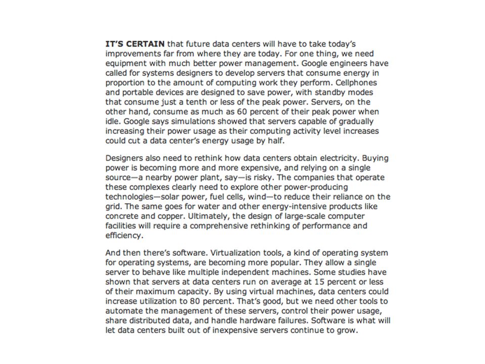
Data Center Design

Similar presentations