Download presentation
Presentation is loading. Please wait.

1
IH2655 Seminar January 26, 2016 Electrical Characterization,B. Gunnar Malm gunta@kth.se

2
Outline Background (material from IH2652 in particular review by Deen) Process flow & measurements (suggested reading) In-line (on-wafer) measurements and test-structures (process-control monitors) Measurement types examples of IV and CV and process stability
 Process flow & measurements (suggested reading) In-line (on-wafer) measurements and test-structures (process-control monitors) Measurement types examples of IV and CV and process stability")
3
Process flow & measurements Monitor starting wafer resistivity Monitor ion-implantations in patterned regions (wells and contacts), requires monitor wafer plus physical methods Monitor gate dielectric stack through IV, CV and reliability measurements Monitor back-end through specific contact resistivity and sheet resistance (interconnects). Also electromigration issues Monitor CD-control, particle contamination Front-end to back-end

4
Process flow & measurements Most of the Chapters in Plummer have a subsection called: Mesurement Methods Electrical measurements 3.4.1.2 Sheet resistance on page 113 4.4.1 Particle control on pages 171-172 5.4.3 Etched features on pages 244-246 6.4.3 The MOS Capacitor on page 301 7.4.3-4 Sheet resistance & Capacitance-Voltage on page 398- (also 2D methods) 11.4.2 Contact resistance/transfer length/oxide breakdown/accel. testing p.726 Front-end to back-end

5
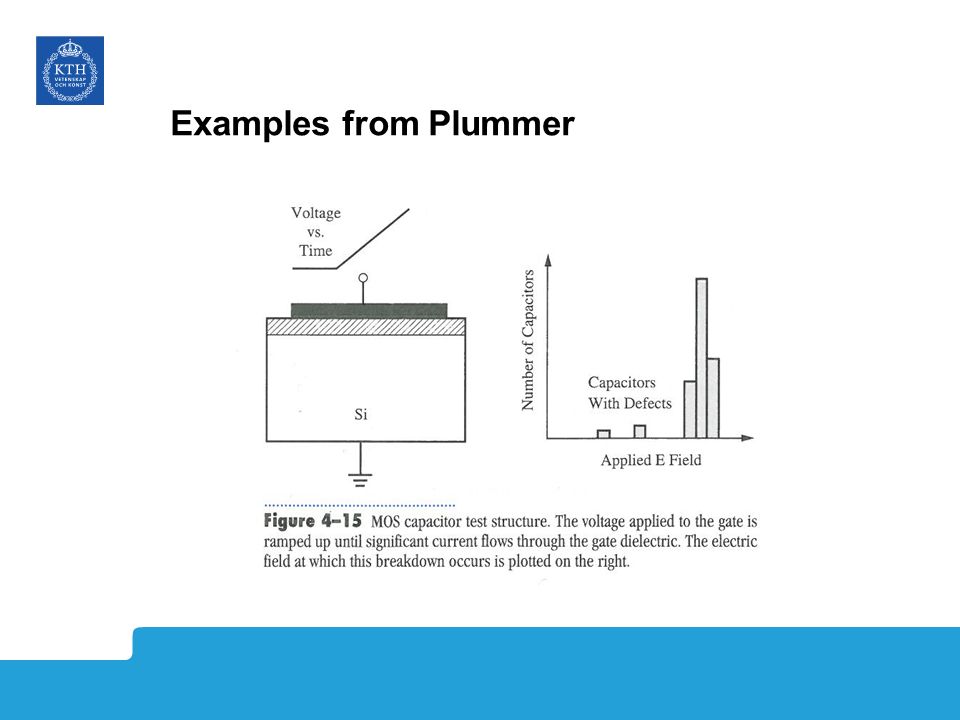
Examples from Plummer

7
Test structures All measurements are typically on a 200-300 mm inch wafer. Map statistics at selected locations Process control monitors located at edge of die (pads in line/row) Special test dies of structures for in-line probe-card measurement (PCM)
 Special test dies of structures for in-line probe-card measurement (PCM).")
8
Device under test (DUT) MOS capacitances for dielectrics 4-terminal resistance structures –Van der Pauw for sheet resistance of metals, silicides, implanted/activated dopants –Cross Bridge Kelvin for contact resistance (metal- to-semiconductor) Different MOSFET transistors (gate length and width)rays
 MOS capacitances for dielectrics 4-terminal resistance structures –Van der Pauw for sheet resistance of metals, silicides, implanted/activated dopants –Cross Bridge Kelvin for contact resistance (metal- to-semiconductor) Different MOSFET transistors (gate length and width)rays")
9
Interconnects needed for electrical probing! http://www.eetimes.com/document.asp?doc_id=1324343

10
Measurement setup Automatic wafer prober http://www.kth.se/ict/forskning/ickretsar/kiselbaserade-kompontenter http://www.kth.se/ict/forskning/ickretsar/kiselbaserade-kompontenter micromanipulators with needle probes or probe cards

11
Test-structure PADS S B G D 4-15 metal layers for interconnects. Top layer thick and soft metal (Al or Au few microns) First metal layer for in-line testing in cleanroom=fab area 80x80 m, pitch m 100
 First metal layer for in-line testing in cleanroom=fab area 80x80 m, pitch m 100.")
12
Array of DUTs vs bonding pads

13
In-line process control monitors Process control monitors located at edge of die (pads in line/row) Common layout serpentine/folded lines
 Common layout serpentine/folded lines")
14
Characterization types IV/DC with source/measure units (SMUs), possibly preamplifiers below 1pA High current (example small resistance of metal/silicide line or contact) Low current (gate and junction leakage, charge pumping) Pulsed to get information about defects and avoid self- heating AC: Impedance and C-V mainly for MOS gate oxide but also channel mobility
, possibly preamplifiers below 1pA High current (example small resistance of metal/silicide line or contact) Low current (gate and junction leakage, charge pumping) Pulsed to get information about defects and avoid self- heating AC: Impedance and C-V mainly for MOS gate oxide but also channel mobility")
15
The 4-point principle (Kelvin) Separate voltage and current
 Separate voltage and current")
16
Test-structure layout for resistance Cross-bridge Kelvin Contact resistance, metal to highly doped silicon or Metal to silicide

17
Test-structure layout for resistance Cross-bridge Kelvin

18
Test-structure layout for resistance Van der Pauw: 2 current terminals + 2 voltage sense terminals, different length of resistor lines Metal or metal silicide lines, approx 10 – 1000

19
Examples from Plummer

20
MOS gate oxide process stability IV - oxide integrity, leakage current, breakdown field, charge-to-breakdown (QDB, TDDB), hot- carrier injection (HCI), stress (NBTI) CV - thickness (TOX), trapped charge, interface states
, hot- carrier injection (HCI), stress (NBTI) CV - thickness (TOX), trapped charge, interface states")
21
The set of CV curves from a wafer contains information about the charge in traps and interface states. Shift with respect to ideal curve shows the type of effect present. Interpretation of real life MOS CV data

22
MOS CV-curves Sweep direction Delta ’Vfb’ hysteresis Shift in Vfb The set of CV curves from a wafer contains information about the charge in traps and interface states and TOX Shift with respect to ideal curve shows the type of effect present

23
How to interpret CV-data

24
Monitoring of process stability Gate length variation - critical dimension (CD) control Monitor gate electrode in 4-point resistor configuration across wafer, plot in Weibull graph
 control Monitor gate electrode in 4-point resistor configuration across wafer, plot in Weibull graph")
25
Examples from Plummer

26
Summary We have followed the process flow and identified need for measurements for starting wafer, front-end and back-end Placement of process control monitors and layout of pads introduced

27
27 L4: Seminar - Concept Test 4.2 Electrical characterization is used to evaluate new materials: Which statements are true? (One or more answers may be correct) A.Capacitance-Voltage (CV) is the best technique to probe defects and thickness of thin oxides B.Current-Voltage (IV) is the best technique to probe defects and thickness of thin oxides C.Both IV and CV are needed to probe defects in thin oxides D.Both IV and CV are needed to probe thickness of thin oxide E.None of the above.
 A.Capacitance-Voltage (CV) is the best technique to probe defects and thickness of thin oxides B.Current-Voltage (IV) is the best technique to probe defects and thickness of thin oxides C.Both IV and CV are needed to probe defects in thin oxides D.Both IV and CV are needed to probe thickness of thin oxide E.None of the above..")
28
Seminar: Electrical Characterization - Concept Test 3.1 3.1 Electrical characterization is an important step in the wafer fabrication flow: Which statements are true? (One or more answers may be correct) 28 A.Measurements are usually done on completed wafers B.Measurements are usually done during the process flow C.Measurements are usually done on special test structures D.Measurements are usually done on transistors E.None of the above.
 28 A.Measurements are usually done on completed wafers B.Measurements are usually done during the process flow C.Measurements are usually done on special test structures D.Measurements are usually done on transistors E.None of the above..")
Similar presentations


>")


