Download presentation
Presentation is loading. Please wait.

1
FPGA and ASIC Technology Comparison - 1 © 2009 Xilinx, Inc. All Rights Reserved ASIC to FPGA Coding Conversion, Part 2

2
Fundamentals of FPGA Design 1 day Designing for Performance 2 day s Advanced FPGA Implementation 2 days Intro to VHDL or Intro to Verilog 3 days FPGA and ASIC Technology Comparison FPGA vs. ASIC Design Flow ASIC to FPGA Coding Conversion Virtex-5 Coding Techniques Spartan-3 Coding Techniques CurriculumPath for ASIC Design FPGA and ASIC Technology Comparison

3
Welcome If you are an experienced ASIC designer transitioning to FPGAs, this course will help you reduce your learning curve by leveraging your ASIC experience Careful attention to how a design can be optimized for an FPGA will help you create a fast and reliable FPGA design

4
Optimize ASIC code for implementation in an FPGA Describe the steps to perform ASIC to FPGA code conversion After completing this module, you will able to:

5
© 2007 Xilinx, Inc. All Rights Reserved FPGA and ASIC Technology Comparison - 5 © 2007 Xilinx, Inc. All Rights Reserved FPGA and ASIC Technology Comparison - 5 © 2009 Xilinx, Inc. All Rights Reserved Code Conversion Steps A ten-step guide to design conversion Step 1: Convert memories (using the CORE Generator™ tool) Step 2: Convert DCMs and PLLs (using the Architecture Wizard) Step 3: Convert SERDES (using the ChipSync Wizard) Step 4: Convert DSP (using the CORE Generator tool) Step 5: Replace IP (using the CORE Generator tool) Step 6: Use the Xilinx SRL (HDL) Step 7: Use clock enables (HDL) Step 8: Employ other good HDL coding styles (HDL) Step 9: Pipeline combinatorial logic (good design practice) Step 10: Build effective finite state machines (HDL)
 Step 2: Convert DCMs and PLLs (using the Architecture Wizard) Step 3: Convert SERDES (using the ChipSync Wizard) Step 4: Convert DSP (using the CORE Generator tool) Step 5: Replace IP (using the CORE Generator tool) Step 6: Use the Xilinx SRL (HDL) Step 7: Use clock enables (HDL) Step 8: Employ other good HDL coding styles (HDL) Step 9: Pipeline combinatorial logic (good design practice) Step 10: Build effective finite state machines (HDL).")
6
© 2007 Xilinx, Inc. All Rights Reserved FPGA and ASIC Technology Comparison - 6 © 2007 Xilinx, Inc. All Rights Reserved FPGA and ASIC Technology Comparison - 6 © 2009 Xilinx, Inc. All Rights Reserved IP Cores Xilinx provides intellectual property cores for your design via the CORE Generator tool Use the CORE Generator tool to generate LogiCORE™ IP LogiCORE IP are supported by Xilinx Some point solution cores have a charge associated, but almost all are FREE Use the CORE Generator tool to find information on AllianceCORE IP AllianceCORE IP are those sold through Alliance partners—third-party vendors All have a charge associated All are supported by third-party vendors

7
© 2007 Xilinx, Inc. All Rights Reserved FPGA and ASIC Technology Comparison - 7 © 2007 Xilinx, Inc. All Rights Reserved FPGA and ASIC Technology Comparison - 7 © 2009 Xilinx, Inc. All Rights Reserved CORE Generator Tool IP Basic elements Counters, comparators, and shift registers DSP functions FIR filters, correlators, modulation, transforms, trig functions, and waveform synthesis Math functions Dividers, floating point module, multipliers, MACs, and square-root generators Memories All combinations of block RAM/ROM, FIFOs, MIG, and CAMs FPGA features ChipSync™ technology, Clocking Wizard, RocketIO GTP Wizard, System Monitor, XtremeDSP slice (more math functions) Standard bus interfaces PCI™, PCI-X™, PCI Express®, and Serial RapidIO technology
 Standard bus interfaces PCI™, PCI-X™, PCI Express®, and Serial RapidIO technology.")
8
© 2007 Xilinx, Inc. All Rights Reserved FPGA and ASIC Technology Comparison - 8 © 2007 Xilinx, Inc. All Rights Reserved FPGA and ASIC Technology Comparison - 8 © 2009 Xilinx, Inc. All Rights Reserved Core Benefits Why use the CORE Generator tool for implementing high-level cores? Cores are pre-tested and use optimum device resources Engineering cost and time can be reduced Some are Relationally Placed Macros (RPMs) providing optimized speed and area results VHDL and Verilog simulation models are provided
 providing optimized speed and area results VHDL and Verilog simulation models are provided.")
9
© 2007 Xilinx, Inc. All Rights Reserved FPGA and ASIC Technology Comparison - 9 © 2007 Xilinx, Inc. All Rights Reserved FPGA and ASIC Technology Comparison - 9 © 2009 Xilinx, Inc. All Rights Reserved Use the SRL Xilinx Virtex®-based FPGAs have the ability to use a LUT as a 16 x 1 shift register (the Virtex-5 FPGA can make a 32 x 1) SRL is used as a pipeline delay element or to capture burst data Serial in and serial out Non-loadable No parallel-in/out Saves flip-flops Saves resources over an ASIC shift-register implementation
 SRL is used as a pipeline delay element or to capture burst data Serial in and serial out Non-loadable No parallel-in/out Saves flip-flops Saves resources over an ASIC shift-register implementation.")
10
© 2007 Xilinx, Inc. All Rights Reserved FPGA and ASIC Technology Comparison - 10 © 2007 Xilinx, Inc. All Rights Reserved FPGA and ASIC Technology Comparison - 10 © 2009 Xilinx, Inc. All Rights Reserved SRL Inference SRLs can be inferred by Synopsys, Mentor, and XST SRLs can also be instantiated by using an SRL primitive or through the CORE Generator tool Use the characterization 1) Synchronous shift 2) Asynchronous read 3) No set or reset functionality VHDL: process (clk) begin if rising_edge(clk) then -- synchronous shift sr <= sr(14 downto 1) & din; end if; end process; -- asynchronous read dout <= sr(15); Verilog: always @ (posedge clk) // synchronous shift sr <= {sr[14:1], din}; // asynchronous read dout <= sr(15);
 Synchronous shift 2) Asynchronous read 3) No set or reset functionality VHDL: process (clk) begin if rising_edge(clk) then -- synchronous shift sr <= sr(14 downto 1) & din; end if; end process; -- asynchronous read dout <= sr(15); Verilog: (posedge clk) // synchronous shift sr <= {sr[14:1], din}; // asynchronous read dout <= sr(15);.")
11
© 2007 Xilinx, Inc. All Rights Reserved FPGA and ASIC Technology Comparison - 11 © 2007 Xilinx, Inc. All Rights Reserved FPGA and ASIC Technology Comparison - 11 © 2009 Xilinx, Inc. All Rights Reserved SRL with Enable Inference Likewise, the SRLE can be inferred VHDL: process (clk) begin if rising_edge(clk) then if en = ‘1’ then -- synchronous shift with enable sr <= sr(14 downto 1) & din; end if; end process; -- asynchronous read dout <= sr(15); Verilog: always @ (posedge clk) if (en) // synchronous shift with enable sr <= {sr[14:1], din}; // asynchronous read dout <= sr(15);
 begin if rising_edge(clk) then if en = ‘1’ then -- synchronous shift with enable sr <= sr(14 downto 1) & din; end if; end process; -- asynchronous read dout <= sr(15); Verilog: (posedge clk) if (en) // synchronous shift with enable sr <= {sr[14:1], din}; // asynchronous read dout <= sr(15);.")
12
© 2007 Xilinx, Inc. All Rights Reserved FPGA and ASIC Technology Comparison - 12 © 2007 Xilinx, Inc. All Rights Reserved FPGA and ASIC Technology Comparison - 12 © 2009 Xilinx, Inc. All Rights Reserved Enhanced Register Virtex-5 registers provide clock enables, synchronous sets, and synchronous resets—directly on the register All three can be used on any register To directly use the pins on the register, the priority must be: Reset, Set, CE By having these pins directly on the register, the fan-in to the LUT is reduced Without a direct pin on the register, these functions would be implemented through the LUT before the register

13
© 2007 Xilinx, Inc. All Rights Reserved FPGA and ASIC Technology Comparison - 13 © 2007 Xilinx, Inc. All Rights Reserved FPGA and ASIC Technology Comparison - 13 © 2009 Xilinx, Inc. All Rights Reserved …………………………. Enhanced Register Example process (clk) begin if rising_edge(clk) then if reset = ‘1’ then -- synchronous reset data ‘0’); elsif set = '1' then -- synchronous set data '1'); elsif ce = '1' then -- clock enable data <= data_in; end if; end process;
 begin if rising_edge(clk) then if reset = ‘1’ then -- synchronous reset data ‘0’); elsif set = 1 then -- synchronous set data 1 ); elsif ce = 1 then -- clock enable data <= data_in; end if; end process;.")
14
© 2007 Xilinx, Inc. All Rights Reserved FPGA and ASIC Technology Comparison - 14 © 2007 Xilinx, Inc. All Rights Reserved FPGA and ASIC Technology Comparison - 14 © 2009 Xilinx, Inc. All Rights Reserved Synchronous Design Replace gated clock circuits with a CE circuit

15
© 2007 Xilinx, Inc. All Rights Reserved FPGA and ASIC Technology Comparison - 15 © 2007 Xilinx, Inc. All Rights Reserved FPGA and ASIC Technology Comparison - 15 © 2009 Xilinx, Inc. All Rights Reserved Clock Enable Circuit always @ (posedge clk) begin count <= count + 1; -- infers a decoded clock enable if (count == 4'b1110) q <= d; end // always @ (posedge clk)
 begin count <= count + 1; -- infers a decoded clock enable if (count == 4 b1110) q <= d; end // (posedge clk).")
16
© 2007 Xilinx, Inc. All Rights Reserved FPGA and ASIC Technology Comparison - 16 © 2007 Xilinx, Inc. All Rights Reserved FPGA and ASIC Technology Comparison - 16 © 2009 Xilinx, Inc. All Rights Reserved Synchronous Reset Synchronous Set and Reset For internal reset circuits, use a synchronous set or reset Similar to the gated clock example, an asynchronous signal that provides a set or reset can glitch, propagating erroneous data Be careful with Global Resets Only one reset port

17
© 2007 Xilinx, Inc. All Rights Reserved FPGA and ASIC Technology Comparison - 17 © 2007 Xilinx, Inc. All Rights Reserved FPGA and ASIC Technology Comparison - 17 © 2009 Xilinx, Inc. All Rights Reserved Synchronous Reset Example process (clk) begin if rising_edge(clk) then count <= count + 1; if count = "1110" then -- synchronous reset q '0'); else q <= d; end if; end process;
 begin if rising_edge(clk) then count <= count + 1; if count = 1110 then -- synchronous reset q 0 ); else q <= d; end if; end process;.")
19
© 2007 Xilinx, Inc. All Rights Reserved FPGA and ASIC Technology Comparison - 19 © 2007 Xilinx, Inc. All Rights Reserved FPGA and ASIC Technology Comparison - 19 © 2009 Xilinx, Inc. All Rights Reserved Inference of Arithmetic Logic Arithmetic logic is implemented by using the dedicated carry chain For access to the dedicated carry chain, the HDL must use arithmetic operators +, –, *, /, >, <, = That is, you will not infer the use of the carry chain by explicitly building the arithmetic logic For example, Half_Sum <= A xor B will not infer the carry chain Half_Sum <= A + B will infer the carry chain

20
© 2007 Xilinx, Inc. All Rights Reserved FPGA and ASIC Technology Comparison - 20 © 2007 Xilinx, Inc. All Rights Reserved FPGA and ASIC Technology Comparison - 20 © 2009 Xilinx, Inc. All Rights Reserved Counters To increase performance, try different types of counters Binary: Slow, familiar count sequence; fewest amount of registers One-hot: Fast; uses the maximum number of registers Johnson: Ring counter; fast and uses fewer registers than one-hot encoding LFSR: Fast, pseudo-random sequence and uses few registers

21
© 2007 Xilinx, Inc. All Rights Reserved FPGA and ASIC Technology Comparison - 21 © 2007 Xilinx, Inc. All Rights Reserved FPGA and ASIC Technology Comparison - 21 © 2009 Xilinx, Inc. All Rights Reserved Decode Logic Example Instead of this… Use case statements for decode logic whenever possible process (clk) begin if rising_edge(clk) then cs0 <= '0'; -- default value cs1 <= '0'; -- default value cs2 <= '0'; -- default value if addr <= "0011" then cs0 <= '1'; elsif (addr > "0011" and addr <= "0111”) then cs1 <= '1'; elsif addr > "0111" then cs2 <= '1'; end if; end process;
 begin if rising_edge(clk) then cs0 <= 0 ; -- default value cs1 <= 0 ; -- default value cs2 <= 0 ; -- default value if addr <= 0011 then cs0 <= 1 ; elsif (addr > 0011 and addr <= 0111 ) then cs1 <= 1 ; elsif addr > 0111 then cs2 <= 1 ; end if; end process;.")
22
© 2007 Xilinx, Inc. All Rights Reserved FPGA and ASIC Technology Comparison - 22 © 2007 Xilinx, Inc. All Rights Reserved FPGA and ASIC Technology Comparison - 22 © 2009 Xilinx, Inc. All Rights Reserved Best Decode Solution …use this Use case statements for decode logic whenever possible process (clk) begin if rising_edge(clk) then cs0 <= '0'; -- default value cs1 <= '0'; -- default value cs2 <= '0'; -- default value case (conv_integer(addr)) is when 0 to 3 => -- x“0000” to x”0011” cs0 <= ‘1’; when 4 to 7 => -- x”0100” to x”0111” cs1 <= ‘1’; when 8 to 15 => -- x”1000” to x”1111” cs2 <= ‘1’; when others => null; end case; end if; end process;
 begin if rising_edge(clk) then cs0 <= 0 ; -- default value cs1 <= 0 ; -- default value cs2 <= 0 ; -- default value case (conv_integer(addr)) is when 0 to 3 => -- x 0000 to x 0011 cs0 <= ‘1’; when 4 to 7 => -- x 0100 to x 0111 cs1 <= ‘1’; when 8 to 15 => -- x 1000 to x 1111 cs2 <= ‘1’; when others => null; end case; end if; end process;.")
23
© 2007 Xilinx, Inc. All Rights Reserved FPGA and ASIC Technology Comparison - 23 © 2007 Xilinx, Inc. All Rights Reserved FPGA and ASIC Technology Comparison - 23 © 2009 Xilinx, Inc. All Rights Reserved High Performance To achieve high performance in FPGAs, you may have to add pipeline delays The biggest issue to consider is latency requirements Remember, the registers exist on the die, and the Xilinx architecture is register rich Note that Virtex-5 does not need as much pipelining You may also need to perform “retiming” Relocating registers to move part of a combinatorial path delay from one side of the register to the other side To increase chip-to-chip performance, register all inputs and outputs of the chip Use the DCM to eliminate clock distribution delays on (and off) chip for decreased chip-to-chip delays
 chip for decreased chip-to-chip delays.")
24
© 2007 Xilinx, Inc. All Rights Reserved FPGA and ASIC Technology Comparison - 24 © 2007 Xilinx, Inc. All Rights Reserved FPGA and ASIC Technology Comparison - 24 © 2009 Xilinx, Inc. All Rights Reserved Increasing Performance Multipliers Use DSP slice multipliers created in the CORE Generator tool Register selector expressions, inputs, and outputs for multiplexers and decoders Register all inputs for multiplexers Register multiple stages of an adder Register inputs and outputs at the top level Increase chip-to-chip performance Register outputs of behavioral sub-blocks Synchronous design methodology

25
© 2007 Xilinx, Inc. All Rights Reserved FPGA and ASIC Technology Comparison - 25 © 2007 Xilinx, Inc. All Rights Reserved FPGA and ASIC Technology Comparison - 25 © 2009 Xilinx, Inc. All Rights Reserved Analyze Delays Analyze the delays on combinatorial paths to determine whether a pipeline delay is required Virtex-5 should use maximum 3 logic levels Other devices should use maximum 4 logic levels But you make your own definition of performance!

26
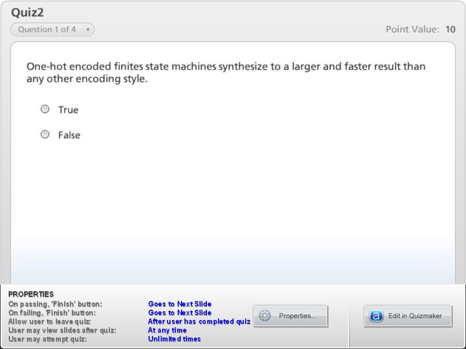
© 2007 Xilinx, Inc. All Rights Reserved FPGA and ASIC Technology Comparison - 26 © 2007 Xilinx, Inc. All Rights Reserved FPGA and ASIC Technology Comparison - 26 © 2009 Xilinx, Inc. All Rights Reserved FSM Encoding Style To achieve high performance for FSMs, consider choosing an alternative encoding style One hot is the most popular, but best to re-synthesize large and complex FSMs for binary and Gray as well FSM Performance depends on… LUT architecture Number of inputs Number of states Desired speed Complexity (number of transitions) Amount of available resources For very large state machines (greater than 32 states), you may want to consider gray-encoding style For small state machines (fewer than four states), binary encoding will generally provide equivalent performance
 Amount of available resources For very large state machines (greater than 32 states), you may want to consider gray-encoding style For small state machines (fewer than four states), binary encoding will generally provide equivalent performance.")
27
© 2007 Xilinx, Inc. All Rights Reserved FPGA and ASIC Technology Comparison - 27 © 2007 Xilinx, Inc. All Rights Reserved FPGA and ASIC Technology Comparison - 27 © 2009 Xilinx, Inc. All Rights Reserved FSM Coding Style Use case statements rather than if-then-else statements Logic will be implemented in parallel, reducing the longest delay path Separate next-state logic from output decoding logic Place next-state decoding logic and output decoding logic in a separate process or always block Prevents the synthesis tool from sharing logic resources, which generally results in less delay but more area Be aware of inadvertent latch or clock-enable inference Use default assignments before the case statement Clock enables are not always bad; however, be careful of lengthy decoding logic for the clock enable

29
© 2007 Xilinx, Inc. All Rights Reserved FPGA and ASIC Technology Comparison - 29 © 2007 Xilinx, Inc. All Rights Reserved FPGA and ASIC Technology Comparison - 29 © 2009 Xilinx, Inc. All Rights Reserved To obtain the desired performance and area goals, the design needs to be optimized for a Xilinx FPGA This will require you following all of our HDL coding recommendations Each synthesis tool requires different resources to be instantiated Know the limitations of your synthesis tools ability to infer resources Use good HDL coding styles (check out the RELs) We finished the ten-step guide to design conversion Step 4: Convert DSP (using the CORE Generator tool) Step 5: Replace IP (using the CORE Generator tool) Step 6: Use the Xilinx SRL (HDL) Step 7: Use clock enables (HDL) Step 8: Employ other good HDL coding styles (HDL) Step 9: Pipeline combinatorial logic (good design practice) Step 10: Build effective finite state machines (HDL) Summary
 We finished the ten-step guide to design conversion Step 4: Convert DSP (using the CORE Generator tool) Step 5: Replace IP (using the CORE Generator tool) Step 6: Use the Xilinx SRL (HDL) Step 7: Use clock enables (HDL) Step 8: Employ other good HDL coding styles (HDL) Step 9: Pipeline combinatorial logic (good design practice) Step 10: Build effective finite state machines (HDL) Summary.")
30
© 2007 Xilinx, Inc. All Rights Reserved FPGA and ASIC Technology Comparison - 30 © 2007 Xilinx, Inc. All Rights Reserved FPGA and ASIC Technology Comparison - 30 © 2009 Xilinx, Inc. All Rights Reserved Where Can I Learn More? Xilinx online documents www.support.xilinx.com Software manuals – Synthesis and Simulation Design Guide – Core Data Sheet (accessible from the Core Generator) » Provides feature description and resource utilization info – Xilinx Unified Libraries Guide Xilinx Training www.xilinx.com/training Virtex-5 FPGA Coding Techniques video (Free) Spartan-3 FPGA Coding Techniques video (Free) Fundamentals of FPGA Design Designing for Performance
 » Provides feature description and resource utilization info – Xilinx Unified Libraries Guide Xilinx Training Virtex-5 FPGA Coding Techniques video (Free) Spartan-3 FPGA Coding Techniques video (Free) Fundamentals of FPGA Design Designing for Performance.")
31
© 2007 Xilinx, Inc. All Rights Reserved FPGA and ASIC Technology Comparison - 31 © 2007 Xilinx, Inc. All Rights Reserved FPGA and ASIC Technology Comparison - 31 © 2009 Xilinx, Inc. All Rights Reserved Xilinx is disclosing this Document and Intellectual Propery (hereinafter “the Design”) to you for use in the development of designs to operate on, or interface with Xilinx FPGAs. Except as stated herein, none of the Design may be copied, reproduced, distributed, republished, downloaded, displayed, posted, or transmitted in any form or by any means including, but not limited to, electronic, mechanical, photocopying, recording, or otherwise, without the prior written consent of Xilinx. Any unauthorized use of the Design may violate copyright laws, trademark laws, the laws of privacy and publicity, and communications regulations and statutes. Xilinx does not assume any liability arising out of the application or use of the Design; nor does Xilinx convey any license under its patents, copyrights, or any rights of others. You are responsible for obtaining any rights you may require for your use or implementation of the Design. Xilinx reserves the right to make changes, at any time, to the Design as deemed desirable in the sole discretion of Xilinx. Xilinx assumes no obligation to correct any errors contained herein or to advise you of any correction if such be made. Xilinx will not assume any liability for the accuracy or correctness of any engineering or technical support or assistance provided to you in connection with the Design. THE DESIGN IS PROVIDED “AS IS" WITH ALL FAULTS, AND THE ENTIRE RISK AS TO ITS FUNCTION AND IMPLEMENTATION IS WITH YOU. YOU ACKNOWLEDGE AND AGREE THAT YOU HAVE NOT RELIED ON ANY ORAL OR WRITTEN INFORMATION OR ADVICE, WHETHER GIVEN BY XILINX, OR ITS AGENTS OR EMPLOYEES. XILINX MAKES NO OTHER WARRANTIES, WHETHER EXPRESS, IMPLIED, OR STATUTORY, REGARDING THE DESIGN, INCLUDING ANY WARRANTIES OF MERCHANTABILITY, FITNESS FOR A PARTICULAR PURPOSE, TITLE, AND NONINFRINGEMENT OF THIRD-PARTY RIGHTS. IN NO EVENT WILL XILINX BE LIABLE FOR ANY CONSEQUENTIAL, INDIRECT, EXEMPLARY, SPECIAL, OR INCIDENTAL DAMAGES, INCLUDING ANY LOST DATA AND LOST PROFITS, ARISING FROM OR RELATING TO YOUR USE OF THE DESIGN, EVEN IF YOU HAVE BEEN ADVISED OF THE POSSIBILITY OF SUCH DAMAGES. THE TOTAL CUMULATIVE LIABILITY OF XILINX IN CONNECTION WITH YOUR USE OF THE DESIGN, WHETHER IN CONTRACT OR TORT OR OTHERWISE, WILL IN NO EVENT EXCEED THE AMOUNT OF FEES PAID BY YOU TO XILINX HEREUNDER FOR USE OF THE DESIGN. YOU ACKNOWLEDGE THAT THE FEES, IF ANY, REFLECT THE ALLOCATION OF RISK SET FORTH IN THIS AGREEMENT AND THAT XILINX WOULD NOT MAKE AVAILABLE THE DESIGN TO YOU WITHOUT THESE LIMITATIONS OF LIABILITY. The Design is not designed or intended for use in the development of on-line control equipment in hazardous environments requiring fail-safe controls, such as in the operation of nuclear facilities, aircraft navigation or communications systems, air traffic control, life support, or weapons systems (“High-Risk Applications”). Xilinx specifically disclaims any express or implied warranties of fitness for such High-Risk Applications. You represent that use of the Design in such High-Risk Applications is fully at your risk. © 2009 Xilinx, Inc. All rights reserved. XILINX, the Xilinx logo, and other designated brands included herein are trademarks of Xilinx, Inc. PCI, PCIe, and PCI Express are trademarks of PCI-SIG and used under license. All other trademarks are the property of their respective owners. Trademark Information
 to you for use in the development of designs to operate on, or interface with Xilinx FPGAs. Except as stated herein, none of the Design may be copied, reproduced, distributed, republished, downloaded, displayed, posted, or transmitted in any form or by any means including, but not limited to, electronic, mechanical, photocopying, recording, or otherwise, without the prior written consent of Xilinx. Any unauthorized use of the Design may violate copyright laws, trademark laws, the laws of privacy and publicity, and communications regulations and statutes. Xilinx does not assume any liability arising out of the application or use of the Design; nor does Xilinx convey any license under its patents, copyrights, or any rights of others. You are responsible for obtaining any rights you may require for your use or implementation of the Design. Xilinx reserves the right to make changes, at any time, to the Design as deemed desirable in the sole discretion of Xilinx. Xilinx assumes no obligation to correct any errors contained herein or to advise you of any correction if such be made. Xilinx will not assume any liability for the accuracy or correctness of any engineering or technical support or assistance provided to you in connection with the Design. THE DESIGN IS PROVIDED AS IS WITH ALL FAULTS, AND THE ENTIRE RISK AS TO ITS FUNCTION AND IMPLEMENTATION IS WITH YOU. YOU ACKNOWLEDGE AND AGREE THAT YOU HAVE NOT RELIED ON ANY ORAL OR WRITTEN INFORMATION OR ADVICE, WHETHER GIVEN BY XILINX, OR ITS AGENTS OR EMPLOYEES. XILINX MAKES NO OTHER WARRANTIES, WHETHER EXPRESS, IMPLIED, OR STATUTORY, REGARDING THE DESIGN, INCLUDING ANY WARRANTIES OF MERCHANTABILITY, FITNESS FOR A PARTICULAR PURPOSE, TITLE, AND NONINFRINGEMENT OF THIRD-PARTY RIGHTS. IN NO EVENT WILL XILINX BE LIABLE FOR ANY CONSEQUENTIAL, INDIRECT, EXEMPLARY, SPECIAL, OR INCIDENTAL DAMAGES, INCLUDING ANY LOST DATA AND LOST PROFITS, ARISING FROM OR RELATING TO YOUR USE OF THE DESIGN, EVEN IF YOU HAVE BEEN ADVISED OF THE POSSIBILITY OF SUCH DAMAGES. THE TOTAL CUMULATIVE LIABILITY OF XILINX IN CONNECTION WITH YOUR USE OF THE DESIGN, WHETHER IN CONTRACT OR TORT OR OTHERWISE, WILL IN NO EVENT EXCEED THE AMOUNT OF FEES PAID BY YOU TO XILINX HEREUNDER FOR USE OF THE DESIGN. YOU ACKNOWLEDGE THAT THE FEES, IF ANY, REFLECT THE ALLOCATION OF RISK SET FORTH IN THIS AGREEMENT AND THAT XILINX WOULD NOT MAKE AVAILABLE THE DESIGN TO YOU WITHOUT THESE LIMITATIONS OF LIABILITY. The Design is not designed or intended for use in the development of on-line control equipment in hazardous environments requiring fail-safe controls, such as in the operation of nuclear facilities, aircraft navigation or communications systems, air traffic control, life support, or weapons systems ( High-Risk Applications ). Xilinx specifically disclaims any express or implied warranties of fitness for such High-Risk Applications. You represent that use of the Design in such High-Risk Applications is fully at your risk. © 2009 Xilinx, Inc. All rights reserved. XILINX, the Xilinx logo, and other designated brands included herein are trademarks of Xilinx, Inc. PCI, PCIe, and PCI Express are trademarks of PCI-SIG and used under license. All other trademarks are the property of their respective owners. Trademark Information.")
Similar presentations