Download presentation
Presentation is loading. Please wait.

1
EE314 IBM/Motorola Power PC620 IBM Power PC 601 Motorola MC68020 Field Effect Transistors

2
Chapter 12: Field Effect Transistors 1.Construction of MOS 2.NMOS and PMOS 3.Types of MOS 4.MOSFET Basic Operation 5.Characteristics

3
The MOS Transistor Polysilicon Aluminum JFET – Junction Field Effect Transistor MOSFET - Metal Oxide Semiconductor Field Effect Transistor n-channel MOSFET (nMOS) & p-channel MOSFET (pMOS)
 & p-channel MOSFET (pMOS)")
4
The MOS Transistor n+ p-substrate Field-Oxide (SiO 2 ) p+ stopper Polysilicon Gate Oxide Drain Source Gate Bulk Contact CROSS-SECTION of NMOS Transistor
 p+ stopper Polysilicon Gate Oxide Drain Source Gate Bulk Contact CROSS-SECTION of NMOS Transistor")
5
Switch Model of NMOS Transistor Gate Source (of carriers) Drain (of carriers) | V GS | | V GS | < | V T | | V GS | > | V T | Open (off) (Gate = ‘0’) Closed (on) (Gate = ‘1’) R on
 Drain (of carriers) | V GS | | V GS | < | V T | | V GS | > | V T | Open (off) (Gate = ‘0’) Closed (on) (Gate = ‘1’) R on")
6
Switch Model of PMOS Transistor Gate Source (of carriers) Drain (of carriers) | V GS | | V GS | > | V DD – | V T | || V GS | < | V DD – |V T | | Open (off) (Gate = ‘1’) Closed (on) (Gate = ‘0’) R on
 Drain (of carriers) | V GS | | V GS | > | V DD – | V T | || V GS | < | V DD – |V T | | Open (off) (Gate = ‘1’) Closed (on) (Gate = ‘0’) R on")
7
MOS transistors Symbols D S G D S G G S DD S G NMOS Enhancement NMOS PMOS Depletion Enhancement B NMOS with Bulk Contact Channel

8
JFET and MOSFET Transistorsor L = 0.5-10 m W = 0.5-500 m SiO 2 Thickness = 0.02-0.1 m Device characteristics depend on L,W, Thickness, doping levels Symbol

9
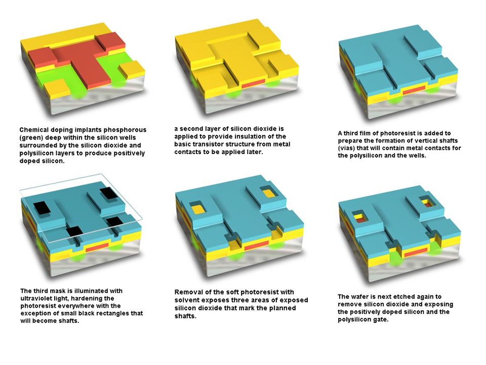
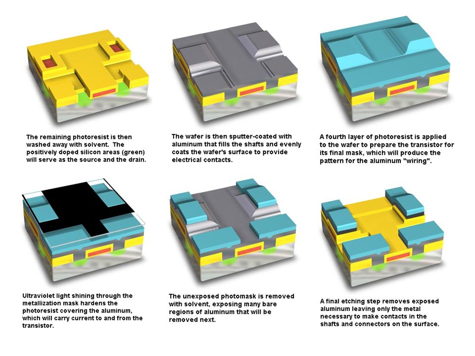
MOSFET Transistor Fabrication Steps

10
Building A MOSFET Transistor Using Silicon http://micro.magnet.fsu.edu/electromag/java/transistor/index.html

14
It is done. Now, how does it work?

15
n-channel MOSFET Basic Operation Operation in the Cutoff region Schematic pn junction: reverse bias i D =0 for v GS < V t0 When v GS =0 then i D =0 until v GS > V t0 (V t0 –threshold voltage)
")
16
n-channel MOSFET Basic Operation Operation in the Triode Region For v DS V t0 the NMOS is operating in the triode region Resistor like characteristic (R between S & D, Used as voltage controlled R) For small v DS, i D is proportional to the excess voltage v GS -V t0
 For small v DS, i D is proportional to the excess voltage v GS -V t0")
17
n-channel MOSFET Basic Operation Operation in the Triode Region Device parameter KP for NMOSFET is 50 A/V 2

18
n-channel MOSFET Basic Operation Operation in the Saturation Region (v DS is increased) Tapering of the channel - increments of i D are smaller when v DS is larger When v GD =V t0 then the channel thickness is 0 and
 Tapering of the channel - increments of i D are smaller when v DS is larger When v GD =V t0 then the channel thickness is 0 and")
19
n-channel MOSFET Basic Operation Example 12.1 An nMOS has W=160 m, L=2 m, KP= 50 A/V 2 and V to =2 V. Plot the drain current characteristic vs drain to source voltage for v GS =3 V.

20
n-channel MOSFET Basic Operation Characteristic Example 12.1 Channel length modulation i d depends on v DS in saturation region (approx: i D =const in saturation region)
")
21
p-channel MOSFET Basic Operation It is constructed by interchanging the n and p regions of n- channel MOSFET. Symbol Characteristic How does p-channel MOSFET operate? -voltage polarities -i D current -schematic

Similar presentations

 Field-Effect Transistors (FET) MOSFET Introduction 1.>")


 Next Week: Review, examples, circuits.>")
![EE415 VLSI Design The Devices: MOS Transistor [Adapted from Rabaey’s Digital Integrated Circuits, ©2002, J. Rabaey et al.]](/16/5062541/big_thumb.jpg "EE415 VLSI Design The Devices: MOS Transistor [Adapted from Rabaey’s Digital Integrated Circuits, ©2002, J. Rabaey et al.]>")

>")
>")


 Importance for LSI/VLSI –Low fabrication cost –Small size –Low power consumption Applications –Microprocessors –Memories.>")


