Download presentation
Presentation is loading. Please wait.

1
CHAPTER 3 Sequential Logic/ Circuits

2
Concept of Sequential Logic Latch and Flip-flops (FFs) Shift Registers and Application Counters (Types, Application & Design) Sequential Circuits Design (State diagram, State Table, K- Map, Circuit)
 Shift Registers and Application Counters (Types, Application & Design) Sequential Circuits Design (State diagram, State Table, K- Map, Circuit)")
3
Sequential vs Combinational Output of any combinational logic circuit depends directly on the input. Generally, in a sequential logic circuit, the output is dependent not only on the input but also on the stored state. Latch is used for the temporary storage of a data bit FF form the basis for most types of sequential logic, such as registers and counters. Also, two types of timing circuits; (1)one-shot and (2) 555 timer
one-shot and (2) 555 timer.")
4
Sequential vs Combinational Combinational circuits. Output determined solely by inputs. Can draw solely with left-to-right signal paths. Sequential circuits. Output determined by inputs XXX previous outputs. Feedback loop. Comb. Cct. input output Seq. Cct. input output

5
Flip-flop & Register Latches Edge-triggered flip-flops Master-slave flip-flops Flip-flop operating characteristics Flip-flop applications One-shots The 555 timer

6
Introduction Latches and FFs are the basic single-bit memory elements used to build sequential circuit with one or two inputs/outputs, designed using individual logic gates and feedback loops. Latches: The output of a latch depends on its current inputs and on its previous output and its change of state can happen at any time when its inputs change. FFs: The output of a flip-flop also depends on current inputs and its previous output but the change of state occurs at specific times determined by a clock input.

7
Latches: D, S-R Latch Gate S-R Latch Gate D-Latch FFs: Edge-Triggered Flip-Flop (S-R, J-K, D) Asynchronous Inputs Master-Slave Flip-Flop Flip-Flop Operating Characteristics Flip-Flop Applications: One-shots & The 555 Timer Introduction A bistable logic circuit that can store a binary 1 or 0 Similar to latch except that it can change state only on the occurrence of one edge of a clock pulse.
 Asynchronous Inputs Master-Slave Flip-Flop Flip-Flop Operating Characteristics Flip-Flop Applications: One-shots & The 555 Timer Introduction A bistable logic circuit that can store a binary 1 or 0 Similar to latch except that it can change state only on the occurrence of one edge of a clock pulse.")
8
Latches Type of temporary storage device that has two stable (bi-stable) states Similar to flip-flop – the outputs are connected back to opposite inputs Main difference from flip-flop is the method used for changing their state Includes: S-R latch, Gated/Enabled S-R latch and Gated D latch
 states Similar to flip-flop – the outputs are connected back to opposite inputs Main difference from flip-flop is the method used for changing their state Includes: S-R latch, Gated/Enabled S-R latch and Gated D latch")
9
S-R (SET-RESET) Latch Active-HIGH input S-R Latch Active-LOW input S-R Latch
 Latch Active-HIGH input S-R Latch Active-LOW input S-R Latch")
10
Logic symbols for the S-R and S-R latch

11
Negative-OR equivalent of the NAND gate S-R latch

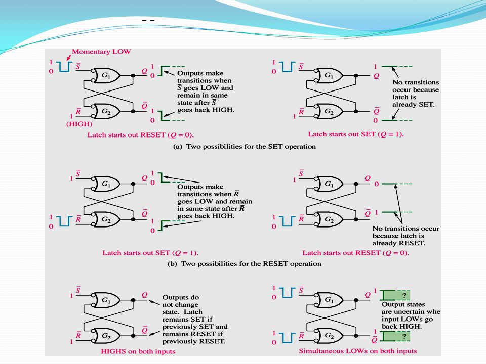
13
Truth table for an active-LOW input S-R latch

14
Assume that Q is initially LOW Waveforms 1345672

15
A gate input is added to the S-R latch to make the latch synchronous. In order for the set and reset inputs to change the latch, the gate input must be active (high/Enable). When the gate input is low, the latch remains in the hold condition. Gated S-R Latch
. When the gate input is low, the latch remains in the hold condition. Gated S-R Latch.")
16
A Gated S-R latch

17
Gated S-R latch waveform: 12345

18
Truth Table for Gated S-R Latch SRGQQ’ 000QQ’Hold 100QQ’Hold 010QQ’Hold 110QQ’hold 001QQ’hold 10110set 01101reset 11100not allowed

19
Gated D Latch (74LS75) The D (data) latch has a single input that is used to set and to reset the flip-flop. When the gate is high, the Q output will follow the D input. When the gate is low, the Q output will hold.

20
Gated S-R Latch Q output waveform if the inputs are as shown: The output follows the input when the gate is high but is in a hold when the gate is low.

21
Gated D Latch (74LS75)
")
22
Edge-triggered Flip-flop Logic Positive edge triggered and Negative edge-triggered All the above flip-flops have the triggering input called clock (CLK/C)
")
23
Clock Signals & Synchronous Sequential Circuits A clock signal is a periodic square wave that indefinitely switches values from 0 to 1 and 1 to 0 at fixed intervals. Rising edges of the clock (Positive-edge triggered) Falling edges of the clock (Negative-edge triggered) Clock signal Clock Cycle Time 1 0
 Falling edges of the clock (Negative-edge triggered) Clock signal Clock Cycle Time 1 0.")
24
Operation of a positive edge-triggered S-R flip-flop (d) S=1, R=1 is invalid or not allowed
 S=1, R=1 is invalid or not allowed")
25
Example:

26
A positive edge-triggered D flip-flop formed with an S-R flip-flop and an inverter. DCLK/CQQ’_________________ 1 ↑10SET (stores a 1) 0 ↑01 RESET (stores a 0)
 0 ↑01 RESET (stores a 0).")
27
Example:

28
Truth Table for J-K Flip Flop JK CLKQQ’ 00Q 0 Q 0 ’ Hold 0101Reset 1010Set 11Q 0 ’Q 0 Toggle (opposite state)
")
29
Transitions illustrating the toggle operation when J =1 and K = 1.

30
The edge-triggered J-K will only accept the J and inputs during the active edge of the clock. The small triangle on the clock input indicates that the device is edge-triggered. A bubble on the clock input indicates that the device responds to the negative edge. no bubble would indicate a positive edge-triggered device. Edge-triggered J-K flip-flop

31
A simplified logic diagram for a positive edge- triggered J-K flip-flop.

32
Example: Positive edge-triggered

33
Example: Negative edge-triggered

34
Preset and Clear Inputs For D, J-K FFs, the inputs are called synchronous input because the state of this inputs control the output only on the triggering edge of clock pulse. (with synch. clock) Most IC FFs also have asynchronous inputs that change the output w/o a clock pulse. (work independently of clock) Two Asynch. Inputs: preset (PRE) and clear (CLR) Some cases called direct set (S D ) and direct reset (R D ) When PRE is active, FF is SET regardless of the When CLR is active, FF is RESET other inputs. Usually, asynch. inputs are active-LOW inputs, indicated with an overbar on the variable & a bubble on the FF symbol
 Most IC FFs also have asynchronous inputs that change the output w/o a clock pulse. (work independently of clock) Two Asynch. Inputs: preset (PRE) and clear (CLR) Some cases called direct set (S D ) and direct reset (R D ) When PRE is active, FF is SET regardless of the When CLR is active, FF is RESET other inputs. Usually, asynch. inputs are active-LOW inputs, indicated with an overbar on the variable & a bubble on the FF symbol.")
35
Logic symbol for a J-K flip-flop with active-LOW preset and clear inputs.

36
Example: Clock pulse 1,2,3 – PRE is LOW, keeping FF SET regardless J-K inputs. Clock pulse 4,5,6,7 - toggle operation occurs b’cos J-K are HIGH and both preset and clear are HIGH (inactive). Clock pulse 8,9 - clear is LOW, keeping FF RESET regardless of J-K inputs.
. Clock pulse 8,9 - clear is LOW, keeping FF RESET regardless of J-K inputs..")
37
The J-K flip-flop has a toggle mode of operation when both J and K inputs are HIGH. Toggle means that the Q output will change states on each active clock edge. J, K and Cp are all synchronous inputs. The master-slave flip-flop is constructed with two latches. The master latch is loaded with the condition of the J-K inputs while the clock is high. When the clock goes low, the slave takes on the state of the master and the master is latched. The master-slave is a level-triggered device. The master-slave can interpret unwanted signals on the J-K inputs. Master-Slave J-K Flip-flop: Edge-triggered flip-flop logic symbols

38
Basic logic diagram for a master-slave J-K flip-flop.

39
Pulse-triggered (master-slave) J-K flip-flop logic symbols.
 J-K flip-flop logic symbols.")
40
Truth Table for Master-Slave J-K Flip Flop JKCLKQQ’ 00Q 0 Q 0 ’ Hold 0101Reset 1010Set 11Q 0 ’Q 0 Toggle (opposite state)
")
41
Flip-Flop Applications Parallel Data Storage Frequency Division Counting

42
Flip-flops used in a basic register for parallel data storage.

43
J-K flip-flop as a divide-by-2 device. Q is one- half the frequency of CLK.

44
Two J-K flip-flops used to divide the clock frequency by 4. Q A is one-half and Q B is one-fourth the frequency of CLK.

45
Flip-flops used to generate a binary count sequence. Two repetitions (00, 01, 10, 11) are shown.
 are shown.")
46
Flip-Flop Operating Characteristics Propagation Delay Times Set-up Time Hold Time Maximum Clock Frequency Pulse Width Power Dissipation

47
Comparison of operating parameters for 4 IC families of flip-flop of the same type

48
There are several other parameters that will also be listed in a manufacturers data sheet. Maximum frequency (F max ) Maximum frequency (F max ) - The maximum frequency allowed at the clock input. Clock pulse width (LOW) [t W (L)] Clock pulse width (LOW) [t W (L)] - The minimum width that is allowed at the clock input during the LOW level. Clock pulse width (HIGH) [t W (H)] Clock pulse width (HIGH) [t W (H)] - The minimum width that is allowed at the clock input during the high level. Set or Reset pulse width (LOW) [t w (L)] Set or Reset pulse width (LOW) [t w (L)] - The minimum width of the LOW pulse at the set or reset inputs.
 Maximum frequency (F max ) - The maximum frequency allowed at the clock input. Clock pulse width (LOW) [t W (L)] Clock pulse width (LOW) [t W (L)] - The minimum width that is allowed at the clock input during the LOW level. Clock pulse width (HIGH) [t W (H)] Clock pulse width (HIGH) [t W (H)] - The minimum width that is allowed at the clock input during the high level. Set or Reset pulse width (LOW) [t w (L)] Set or Reset pulse width (LOW) [t w (L)] - The minimum width of the LOW pulse at the set or reset inputs..")
49
Basic operation of a 555 Timer Threshold Control Voltage Trigger Discharge Reset Output

50
Functional Diagram of 555 Timer

51
555 Timer as a one shot t w = 1.1R1C1 = 1.1(2000 )(1 F) = 2.2ms
(1 F) = 2.2ms")
52
Astable operation of 555 Timer t H =.7 (R1+R2)C1 =2.1ms t L =.7R2C1 = 0.7ms
C1 =2.1ms t L =.7R2C1 = 0.7ms")
Similar presentations


 S – R Latch “Cross-Coupling” two NAND gates gives the S -R Latch:>")


 latches S-R (Set-Reset) Latch.>")


 latches>")


 Department of Computer Science Faculty.>")
