Download presentation
Presentation is loading. Please wait.

1
UNIT-III CONTROL UNIT DESIGN
INTRODUCTION CONTROL TRANSFER FETCH CYCLE INSTRUCTION INTERPRETATION AND EXECUTION HARDWIRED CONTROL MICROPROGRAMMED CONTROL

2
Controller functions Fetch and instruction sequencing (fetch cycle)-Generates control signal to fetch instruction from memory and the sequence of operations involved in processing an instruction Instruction interpretation and execution (execution cycle)-Tasks involved are Interpreting the operand addressing mode implied in the operation code and fetching the operands Sequencing the successive micro operations on the data path to execute the operation code specified in the instruction
-Generates control signal to fetch instruction from memory and the sequence of operations involved in processing an instruction. Instruction interpretation and execution (execution cycle)-Tasks involved are. Interpreting the operand addressing mode implied in the operation code and fetching the operands. Sequencing the successive micro operations on the data path to execute the operation code specified in the instruction.")
3
3. Interrupt processing (interrupt cycle)-Process unmasked interrupt
3.Interrupt processing (interrupt cycle)-Process unmasked interrupt. Tasks are Suspend execution of current program Save context Set PC to start address of interrupt handler routine Process interrupt Restore context and continue interrupted program
-Process unmasked interrupt. Tasks are. Suspend execution of current program. Save context. Set PC to start address of interrupt handler routine. Process interrupt. Restore context and continue interrupted program.")
4
CONTROL TRANSFER Instruction Control Transfer Program Control Transfer

5
CONTROL TRANSFER F E Comments Not used 1 Fetch Cycle Execute Cycle
CPU fetches and executes each instruction of the program Successively goes through fetch, execute and interrupt cycles Two flip-flops marked F and E identify each of these 3 cycles Two general operations Instruction control transfer Program control transfer CPU Cycles F E Comments Not used 1 Fetch Cycle Execute Cycle Interrupt Cycle

6
Instruction Control Transfer

7
Instruction Control Transfer
PC holds the address of the instruction to be executed During fetch cycle PC is incremented to hold the address of the next instruction Assuming each instruction has a length of one word, then PC incremented by one, that is,PC <= PC + 1; Length of a variable length instruction needs to be specified in some bits of the operation code field of instruction Transfer of control to non sequential instruction occurs during execution cycle of conditions branch with specified condition satisfied or by an unconditional branch instruction

8
Example Jump X (Unconditional branch to X) or Jump ZX (Branch to X if the result of last arithmetic operation is zero)
 .")
9
PROGRAM CONTROL TRANSFER

10
PROGRAM CONTROL TRANSFER
While program P1 is running ,CPU is under control of P1 Transfer of program control may occur in 2 situations 1. There is an instruction in P1 which calls a subroutine denoted as program P2 JMPSUBX, where X denotes starting address of P2 2. While an instruction in P1 is getting fetched and executed ,an interrupt flag gets set, where X denotes starting address of ISR(P2).After execution of current instruction branch to location X takes place Prior to transferring control to P2 ,the CPU status of P1 is stored in stack (push and pop operation) Pg-330 2nd para pal chaudhuri book explaination
.After execution of current instruction branch to location X takes place. Prior to transferring control to P2 ,the CPU status of P1 is stored in stack (push and pop operation) Pg-330 2nd para pal chaudhuri book explaination.")
11
FETCH CYCLE

12
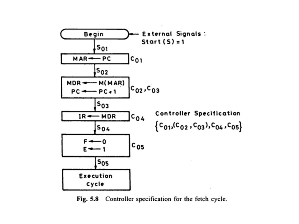
FETCH CYCLE The instruction whose address is determined by the PC is obtained from the memory Loaded into the IR. The PC is then incremented to point to the next instruction and switch over to execution cycle CPU enters fetch cycle if F=1 and E=0 C01: MAR PC C02C03:MDR M(MAR);PC PC+1 C04:IR MDR C05:F 0; E 1 Sequence of micro operations of fetch cycle
;PC PC+1. C04:IR MDR. C05:F 0; E 1. Sequence of micro operations of fetch cycle.")
13
INSTRUCTION INTERPRETATION AND EXECUTION

14
INSTRUCTION INTERPRETATION AND EXECUTION
Instruction loaded into Instruction Register (IR) Processor interprets instruction and performs required actions Different for each instruction e.g. ADD X, R1 - add the contents of location X to Register 1 , result in R1 C61: MAR <- (IRaddress) C62: MDR <- (memory) C63: R1 <- R1 + (MDR) Note no overlap of micro-operations
 Processor interprets instruction and performs required actions. Different for each instruction. e.g. ADD X, R1 - add the contents of location X to Register 1 , result in R1. C61: MAR <- (IRaddress) C62: MDR <- (memory) C63: R1 <- R1 + (MDR) Note no overlap of micro-operations.")
15
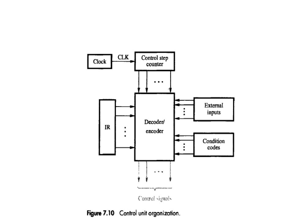
Input-Output behavior of a control unit
Set of signals Cin1 input to the controller from the datapath includes those from the operation code of IR, various flag registers of ALU,interrupt , etc. Other input signals Cin2 are those control which control the operation of the controller itself, such as start, stop, clock, etc. Cout1 fed at appropriate point on the data path to sequence and control the micro operations associated with operation code Other control signal Cout2 cover signals such as busy, operation complete, etc transmitted to other control units Data Path Cin2 Cout2 Control Unit

16
Input-Output behavior of a control unit
Data Path Cin1 Cout1 Cin2 Cout2 Control Unit

17
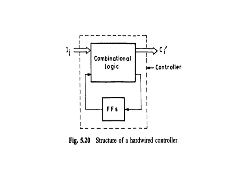
HARDWIRED CONTROL

18
HARDWIRED CONTROL The controller is designed as a sequential logic circuit which generates the specific sequence of control signals as its primary output The sequence of 4 control signals C0, C1, C2, C3 can be developed by using a 2-bit sequence counter C0=C01: MAR PC C1=C02C03:MDR M(MAR);PC PC+1 C2=C04:IR MDR C3=C05:F 0; E 1 Sequence of micro operations of fetch cycle Its output is decoded to derive the desired control signals in the given sequence.
;PC PC+1. C2=C04:IR MDR. C3=C05:F 0; E 1. Sequence of micro operations of fetch cycle. Its output is decoded to derive the desired control signals in the given sequence.")
19
Refer hamacher book page:425 to 429
Must for exam refer ur notes + hamacher book content for above page number

21
Methods for systematic design of hardwired control logic
Sequence counter method: To design controller of moderate complexity Delay element method: Depends on the use of clocked delay elements for generating the sequence of control signals State table method: Employs the algorithmic approach to sequential circuit design using classical state table method

23
Controller specification for the Fetch Sequence
Address of next instruction is in PC (s01) Content of PC loaded into MAR (c01) ,s02 Address (MAR) is placed on address bus Control unit issues READ command Result (data from memory) appears on data bus Data from data bus copied into MDR (Co2),s03 PC incremented by 1 (in parallel with data fetch from memory) (c03),s03 Data (instruction) moved from MDR to IR (c04), S04 MDR is now free for further data fetches (F 0 ; E 1) (c05) , s05
 Content of PC loaded into MAR (c01) ,s02. Address (MAR) is placed on address bus. Control unit issues READ command. Result (data from memory) appears on data bus. Data from data bus copied into MDR (Co2),s03. PC incremented by 1 (in parallel with data fetch from memory) (c03),s03. Data (instruction) moved from MDR to IR (c04), S04. MDR is now free for further data fetches (F 0 ; E 1) (c05) , s05.")
24
Sequence counter method

25
Sequence counter method
Step 1: Identify the distinct phases in the flowchart. Employ log p number of flip flops to handle p number distinct phases Start R 1 Modulo –K counter End S Reset Clock Reset ….. Step 2: Identify the maximum number of distinct steps, k, in each of the phases .Employ a mod k counter to generate control signals for each of the k steps Step 3 : design a combinational logic circuit to generate the sequence of control signals to control the micro operations of each phase I/k Decoder …… c1c ck

26
Delay element method

27
Delay element method Control unit based on delay element method for the fetch cycle Ci,j Begin C01: MAR PC; (d1=t1-t0) t0 Delay block Di D1 C02: MDR M(MAR), c03: PC PC+1 ; (d2=t2-t1) t1 Ci+1,j’ D2 t2 C04: IR MDR; (d3=t3-t2) D3 t3 C05: F 0; E ; (d4=t4-t3) D4 t4 Execute
 t0. Delay block Di. D1. C02: MDR M(MAR), c03: PC PC+1 ; (d2=t2-t1) t1. Ci+1,j’ D2. t2. C04: IR MDR; (d3=t3-t2) D3. t3. C05: F 0; E 1; (d4=t4-t3) D4. t4. Execute.")
29
State table method

30
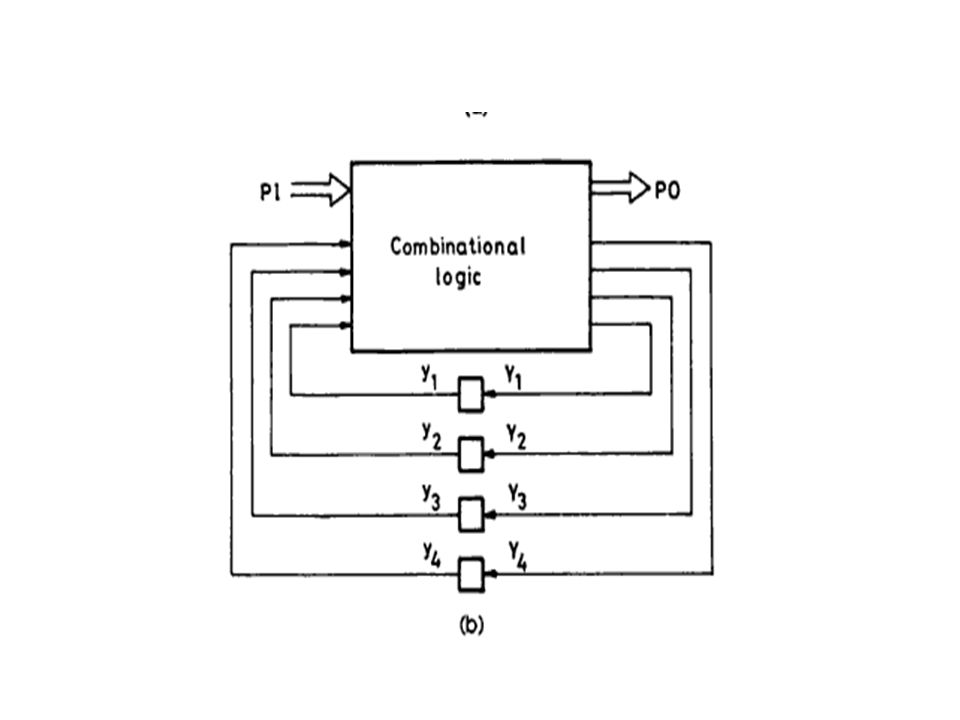
State table method The state Si (i=1,2…) has been marked above each block of the flowchart. state of the controller which generates the control signals to control the micro operations in the data path

33
Steps to design the Control structure realizing flowchart
State Assignment: States are assigned as s1,s2,s3…;each such assignment specifies a particular state of the controller at the specific time step. State table derived from state assignment State Minimization: A set of states {Sa,Sb,…Sc} can be merged to a single state S’ if Si & Sj is pair wise compatible State Encoding: State variables are defined and states are encoded in terms of state variables

34
Hard-wired Control Unit- advantages
1. Minimizes the average number of clock cycles needed per instruction 2. occupies a relatively small area (of the CPU chip area 3. High efficiency in terms of operation speed 4. is to minimize cost of the circuit

35
Problems With Hard Wired Designs
Inflexible design Large design turn around time for complex design Difficult to add new instructions

Similar presentations


 Processor Internals CHAPTER 15: CONTROL UNIT OPERATION 1.>")


