Download presentation
Presentation is loading. Please wait.

1
Multicore Designs Presented By: Mahendra B Salunke Asst. Professor, Dept of Comp Engg., SITS, Narhe, Pune. URL: www.microsig.webs.com

2
Contents Intel 64bit Architecture: ◦ Block Diagram, ◦ Basic Execution Environment, ◦ Data Types, ◦ Specific advances: Instruction set, Intel Micro-architecture code name Nehalem, SIMD Instructions, Hyper threading Technology, Virtualization Technology (Refer TB3) Systems Programming, Multiple Processor Management (Refer RB1)
 Systems Programming, Multiple Processor Management (Refer RB1)")
3
Brief History 16-bit Processors and Segmentation (1978) The Intel® 286 Processor (1982) The Intel386™ Processor (1985): First IA-32 The Intel486™ Processor (1989) The Intel® Pentium® Processor (1993) The P6 Family of Processors (1995-1999) ◦ Intel Pentium Pro processor ◦ Intel Pentium II processor ◦ Pentium II Xeon processor ◦ Intel Celeron processor ◦ Intel Pentium III processor ◦ Pentium III Xeon processor
 The Intel® 286 Processor (1982) The Intel386™ Processor (1985): First IA-32 The Intel486™ Processor (1989) The Intel® Pentium® Processor (1993) The P6 Family of Processors ( ) ◦ Intel Pentium Pro processor ◦ Intel Pentium II processor ◦ Pentium II Xeon processor ◦ Intel Celeron processor ◦ Intel Pentium III processor ◦ Pentium III Xeon processor")
4
Brief History Continued… The Intel® Pentium® 4 Processor Family (2000- 2006) The Intel® Xeon® Processor (2001- 2007) The Intel® Pentium® M Processor (2003-Current) The Intel® Pentium® Processor Extreme Edition (2005-2007): First Intel 64bit The Intel® Core™ Duo and Intel® Core™ Solo Processors (2006-2007) The Intel® Xeon® Processor 5100, 5300 Series and Intel® Core™2 Processor Family (2006-Current) The Intel® Xeon® Processor 5200, 5400, 7400 Series and Intel® Core™2 Processor Family (2007-Current) The Intel® Atom™ Processor Family (2008-Current)
 The Intel® Xeon® Processor ( ) The Intel® Pentium® M Processor (2003-Current) The Intel® Pentium® Processor Extreme Edition ( ): First Intel 64bit The Intel® Core™ Duo and Intel® Core™ Solo Processors ( ) The Intel® Xeon® Processor 5100, 5300 Series and Intel® Core™2 Processor Family (2006-Current) The Intel® Xeon® Processor 5200, 5400, 7400 Series and Intel® Core™2 Processor Family (2007-Current) The Intel® Atom™ Processor Family (2008-Current)")
5
Brief History Continued… The Intel® Core™i7 Processor Family (2008-Current) The Intel® Xeon® Processor 7500 Series (2010) 2010 Intel® Core™ Processor Family (2010) The Intel® Xeon® Processor 5600 Series (2010) Second Generation Intel® Core™ Processor Family (2011)
 The Intel® Xeon® Processor 7500 Series (2010) 2010 Intel® Core™ Processor Family (2010) The Intel® Xeon® Processor 5600 Series (2010) Second Generation Intel® Core™ Processor Family (2011)")
6
Block Diagram

7
Architecture Overview The processor instruction set architecture is designed to achieve a large degree of instruction level parallelism by using speculation and predication. There are two types of speculation: ◦ Control speculation is the execution of an operation before the condition governing its execution. ◦ Data speculation refers to the execution of a memory load prior to a store that might change its value.

8
Continued…. Predication is the conditional execution of instructions that removes branches used for conditional execution eliminating associated miss-predict penalties. Predication and speculation work together to give the compiler a significantly increased scheduling scope across which performance optimizations can be performed more effectively.

9
Continued…. The hardware resources are exposed to the compiler in this explicitly parallel instruction computing (EPIC) machine. Each memory load and store has a 2-bit cache hint field in which the compiler encodes its prediction of the spatial and temporal locality of the memory area being accessed. The processor uses this information to determine the placement of cache lines in the cache hierarchy.
 machine. Each memory load and store has a 2-bit cache hint field in which the compiler encodes its prediction of the spatial and temporal locality of the memory area being accessed. The processor uses this information to determine the placement of cache lines in the cache hierarchy..")
10
Continued…. The branch prediction table (BPT) contains 512 entries and uses a two-level adaptive algorithm. Each entry tracks the four most recent occurrences of that branch. The processor hardware is organized into a ten-stage core pipeline, shown in figure below, that can execute up to six IA-64 instructions in parallel each clock.
 contains 512 entries and uses a two-level adaptive algorithm. Each entry tracks the four most recent occurrences of that branch. The processor hardware is organized into a ten-stage core pipeline, shown in figure below, that can execute up to six IA-64 instructions in parallel each clock..")
11
Continued…. Ten-stage core pipeline

12
Continued…. The first three pipeline stages perform the instruction fetch and deliver the instructions into a decoupling buffer that enables the front-end of the machine to operate independently from the back-end, by allowing the front end to speculatively fetch ahead and by hiding the instruction cache and branch prediction latencies.

13
Continued…. Dispersal and register renaming are performed in the next two stages. Operand delivery is accomplished across the WLD and REG stages, where the register file is accessed and data is delivered through the bypass network after processing the predicate control. Finally, the last three stages perform the wide parallel execution followed by exception management and retirement.

14
Continued…. The processor has 15 execution units: four integer, four multimedia, two floating point, three branch and two load/store units. The processor implements 128 integer and 128 floating point registers, 64 one- bit predicate registers and eight branch registers.

15
Continued…. The processor includes three levels of cache organized in a hierarchical manner. The L1 and L2 caches are integrated on die. At the first level, instruction and data caches are split, each 16kB in size, four-way set- associative and with a 32-byte line size. The second level of cache is unified, 96 kB in size, six-way set-associative and with a 64- byte line size.

16
Continued…. The L3 cache contains up to 4 MB of custom designed on-cartridge memory and is accessed through a dedicated 128- bit BSB source-synchronous interface running at the processor’s core frequency. The L3 cache is four-way set-associative with a line size of 64 bytes.

17
Continued…. Both L2 and L3 caches are completely error correction code (ECC) protected. To enable software-guided optimal utilization of the cache hierarchy, the processor uses a set of memory locality hints that indicate the temporal locality of each access at each level of hierarchy. The processor uses these hints to determine the allocation and replacement strategies for each level of cache. In addition, the processor uses a bias hint to indicate that the software intends to modify the data of a given cache line.

18
Continued…. The floating-point unit delivers up to 6.4 Gflops and provides full support for single, double, extended, and mixed-mode precision computations. Parallel IA-64 FP instructions which operate on pairs of 32-bit single precision numbers increase the single-precision FP computation throughput. The chip also supports multimedia instructions that treat the general registers as vectors of eight 8-bit, four 16-bit, or two 32-bit elements.

19
Continued…. The floating-point execution units support simultaneous multiply-add to provide performance for scientific computation.

20
Continued…. The processor includes special hardware support to ensure full binary compatibility with the IA-32 instruction set. The dynamic out-of-order scheduler optimizes performance on legacy binaries. Shared caches and execution resources increase the area efficiency. The processor can run a mix of IA-32 and IA-64 applications on an IA-64 operating system, as well as IA-32 applications on an IA-32 operating system, in both uni-processor and multi- processor configurations.

21
Continued…. The processor implements a machine check architecture (MCA) that provides the ability to Continue, Recover, or Contain detected errors. All significant structures on the chip are protected by parity or ECC.
 that provides the ability to Continue, Recover, or Contain detected errors. All significant structures on the chip are protected by parity or ECC..")
22
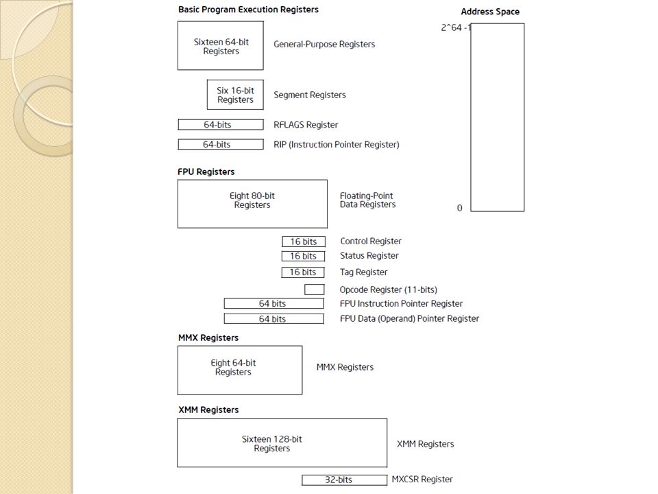
Basic Execution Environment Describes how the processor executes instructions and how it stores and manipulates data. The execution environment described here includes memory (the address space), general-purpose data registers, segment registers, the flag register, and the instruction pointer register.
, general-purpose data registers, segment registers, the flag register, and the instruction pointer register..")
23
MODES OF OPERATION The operating mode determines which instructions and architectural features are accessible The IA-32 architecture supports three basic operating modes: ◦ protected mode, ◦ real-address mode, and ◦ system management mode.

24
Protected mode This mode is the native state of the processor. Among the capabilities of protected mode is the ability to directly execute “real-address mode” 8086 software in a protected, multi- tasking environment. This feature is called virtual-8086 mode, although it is not actually a processor mode. Virtual-8086 mode is actually a protected mode attribute that can be enabled for any task.

25
Real-address mode This mode implements the programming environment of the Intel 8086 processor with extensions (such as the ability to switch to protected or system management mode). The processor is placed in real-address mode following power-up or a reset.

26
System management mode (SMM) This mode provides an operating system or executive with a transparent mechanism for implementing platform- specific functions such as power management and system security. The processor enters SMM when the external SMM interrupt pin (SMI#) is activated or an SMI is received from the advanced programmable interrupt controller (APIC).
 is activated or an SMI is received from the advanced programmable interrupt controller (APIC)..")
27
SMM Continued…. In SMM, the processor switches to a separate address space while saving the basic context of the currently running program or task. SMM-specific code may then be executed transparently. Upon returning from SMM, the processor is placed back into its state prior to the system management interrupt. SMM was introduced with the Intel386™ SL and Intel486™ SL processors and became a standard IA-32 feature with the Pentium processor family.

28
Intel® 64 Architecture (2.2.10) Intel 64 architecture increases the linear address space for software to 64 bits and supports physical address space up to 40 bits. The technology also introduces a new operating mode referred to as IA-32e mode. IA-32e mode operates in one of two sub-modes: ◦ Compatibility mode enables a 64-bit operating system to run most legacy 32-bit software unmodified, ◦ 64-bit mode enables a 64-bit operating system to run applications written to access 64-bit address space.

29
In the 64-bit mode, Applications may access: 64-bit flat linear addressing 8 additional general-purpose registers (GPRs) 8 additional registers for streaming SIMD extensions (SSE, SSE2, SSE3 and SSSE3) 64-bit-wide GPRs and instruction pointers uniform byte-register addressing fast interrupt-prioritization mechanism a new instruction-pointer relative-addressing mode
 8 additional registers for streaming SIMD extensions (SSE, SSE2, SSE3 and SSSE3) 64-bit-wide GPRs and instruction pointers uniform byte-register addressing fast interrupt-prioritization mechanism a new instruction-pointer relative-addressing mode")
31
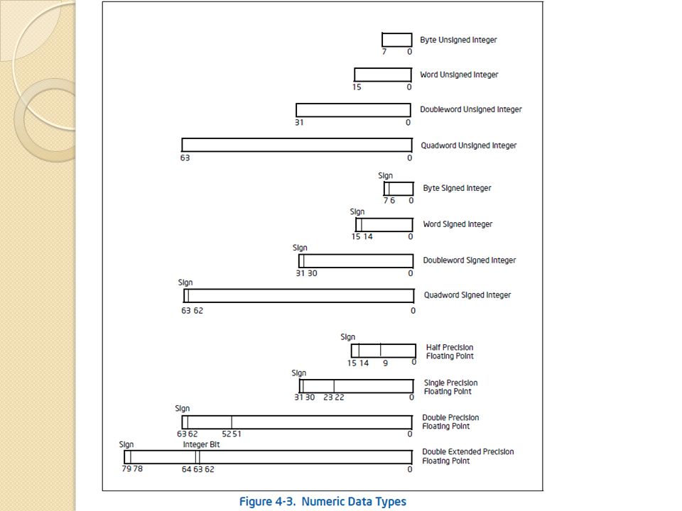
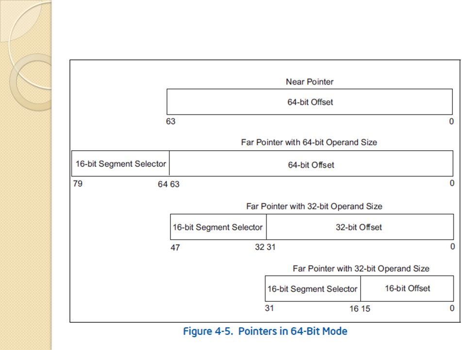
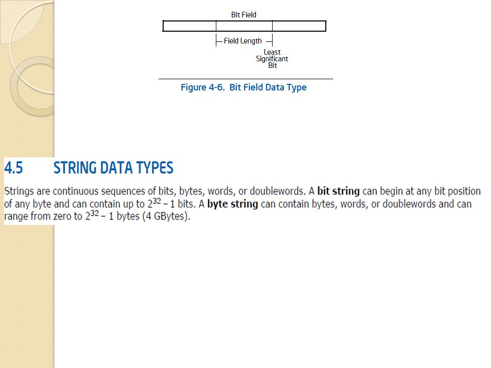
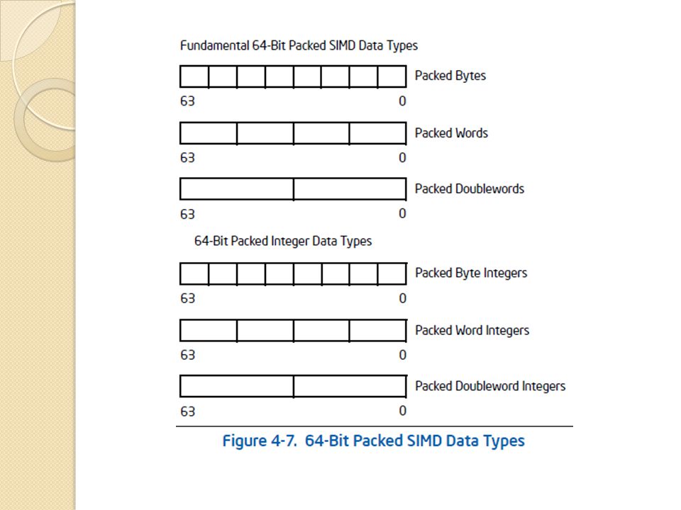
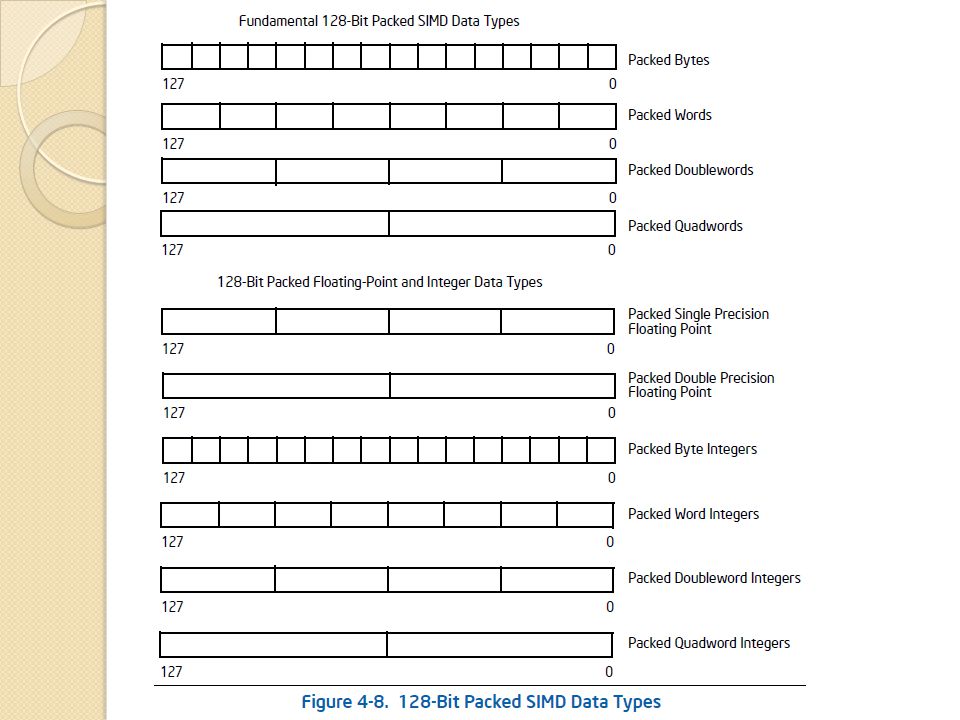
Data Types

39
Reference Intel® 64 and IA-32 Architectures Software Developer’s Manual Volume 1: Basic Architecture 253665.pdf

Similar presentations