Download presentation
Presentation is loading. Please wait.

1
DSP in FPGA

2
Topics Considerations Routing Challenge Paper Analysis
When not to use Floating Point Example FP: Adder Hardware Circuit Constant Cache Data-path with Constant Cache FFT Example Other Examples: Simulink Equalizer Routing Challenge Routing Resources: Altera vs. Xilinx Example: Matrix Multiplication Hypothesis and Rule’s of Thumb Results Paper Analysis Signal Processing FPGA Applications with DSP DSP milestones PDSP Architecture PDSP vs FPGA Example: FIR Filter DSP on FPGA State of the Art Flexibility Multi-Channel Friendly Resources DSP Slice Multiplication Modes IP Blocks IP Block Example: FIR Filter

3
Signal Processing Transform or manipulate analog or digital signal.
Most frequent application: filtering. DSP has replaced related traditional analog signal processing systems in many applications. Historically, ANALOG CHIPS design yielded SMALLER die Size DSP systems are insensitive to change in temperature, aging, or component tolerance. Now, with noise associated with submicrometer designs, Digital designs can be much more densely integrated than analog designs. yield compact, low-power, low-cost digital designs.

4
FPGA’s Applications Data communications, speech, audio, biomedical signal processing, instrumentation, robotics. Speech Processing – coding and decoding, echo cancellation, cochlea-implant signal processing…

5
Efficient algorithm to compute the discrete Fourier Transform (DFT)
Milestones Cooley and Tukey 1965 PDSP 1970 Efficient algorithm to compute the discrete Fourier Transform (DFT) Compute (fixed-point) “multiply-and-accumulate” in only one clock cycle One is the disclosure by Cooley and Tuckey in 1965 of an efficient algorithm to compute the Discrete Fourier Transform. The other milestone was the introduction of the programmable digital signal processor (PDSP) in late 70s. This could compute a (Fixed-point) “multiply-and-accumulate” in only one clock cycle, which was an essential improvement compared with the “Von Neuman” microprocessor based systems in those days. Today PDSPs: Floating-point multipliers, barrel shifters, memory banks, zero-overhead interfaces to A/D and D/A Converters
 Compute (fixed-point) multiply-and-accumulate in only one clock cycle. One is the disclosure by Cooley and Tuckey in 1965 of an efficient algorithm to compute the Discrete Fourier Transform. The other milestone was the introduction of the programmable digital signal processor (PDSP) in late 70s. This could compute a (Fixed-point) multiply-and-accumulate in only one clock cycle, which was an. essential improvement compared with the Von Neuman microprocessor based systems in those days. Today PDSPs: Floating-point multipliers, barrel shifters, memory banks, zero-overhead interfaces to A/D and D/A Converters.")
6
PDSP Architecture Single-DSP implementations have insufficient processing power for today’s system’s complexity. Multiple-chip systems: more costly, complex and higher power requirements. Solution: FPGAs Single DSP implementation: insufficient processing power for complexity of algorithms. System architects can’t afford cost, complexities and power requirements of MULTIPLE CHIP Systems. Traditional DSProceros are MICROPROSESORS deisgned to perform a specialized purpose. They are well-suited to algorithmic-intensive tasks but are limited in PERFORMANCE by CLOCK RATE and Sequential Nature of internal design. This limits the maximum number of operations per second that they can carry out on the incoming data samples. Typically, three or four clock cycles are required per arithmetic logic unit (ALU) operation. Multicore architectures may increase performance, but these are still limited. Designing with traditional DSProcessors therefore necessitates the RESUSE of ARCHitectural ELEMENTS for Alg Impl. Every operation must cycle through the ALU, fed back internally or externally, for each addition, multiplication, subtraction or other fundamental op Every operation must cycle through the ALU, either fed back internally or externally, for each addition, multiplication, subtraction or any other fundamental operation performed. control logic can be implemented in the hardware. Precious clock cycles will not be used implementing control functionality. V.g. using multiple ALUs within a device or multiple DSP devices on a board; however, such schemes often increase costs significantly and simply shift the problem to another arena --- Inreasing performance in mult. Dev. Follows exponentail curve (double, 2, double, 4.. --- Focus of programmers shifts from signal-processing functions to task scheduling across the multiple processors and cores. This results in much additional code that functions as SySTEM OVERHEAD rather than attacking the digital signal-processing problem at hand.
 operation. Multicore architectures may increase performance, but these are still limited. Designing with traditional DSProcessors therefore necessitates the RESUSE of ARCHitectural ELEMENTS for Alg Impl. Every operation must cycle through the ALU, fed back internally or externally, for each addition, multiplication, subtraction or other fundamental op. Every operation must cycle through the ALU, either fed back internally or externally, for each addition, multiplication, subtraction or any other fundamental operation performed. control logic can be implemented in the hardware. Precious clock cycles will not be used implementing control functionality. V.g. using multiple ALUs within a device or multiple DSP devices on a board; however, such schemes often increase costs significantly and simply shift the problem to another arena. --- Inreasing performance in mult. Dev. Follows exponentail curve (double, 2, double, Focus of programmers shifts from signal-processing functions to task scheduling across the multiple processors and cores. This results in much additional code that functions as SySTEM OVERHEAD rather than attacking the digital signal-processing problem at hand.")
7
Managing Resources & Design Reliability
Each task often requires unrestricted access to many processor resources in order to run efficiently. --- to mprove Processing efficiency and DETERMINISTIC LATENCY. --Result: minimal or zero OS isolation between tasks. Vendors try to create different levels of protection or isolation between tasks or threads. The OS or kernel is used to manage access to the processor resources, such as allowable execution time, memory, or common peripheral resources. This to avoid the following problems (mention one or two): ■ Failure of interrupts to completely restore processor state upon completion ■ Undetected corruption or non-initialization of pointers ■ Failing to properly initialize or disable circular buffering addressing modes ■ Memory leaks, the gradual consumption of available volatile memory due to failure of a thread to release all memory when finished ■ Dependency of DSP routines on specific memory arrangements of variables ■ Pipeline restrictions of some assembly instructions ■ Non-uniform assumptions regarding processor resources by multiple engineers simultaneously developing and integrating disparate functions ■ Blocking of critical interrupt by another interrupt or by an uninterruptible process ■ Unexpected memory rearrangement by optimizing memory linkers and compliers■ Use of special DSP “core mode” instruction options in core ■ Conflict or excessive latency between peripheral accesses, such as DMA, serial ports, L1, L2, and external SDRAM memories ■ Corrupted stack or semaphores ■ Subroutine execution times dependent on input data or configuration ■ Mixture of “C” or high-level language subroutines with assembly language subroutines Near Impossible to test all the CORNER Casses (permutations) and interactions between diferent Tasks or Threads. challenge during software develop. ================ ON FPGA, The complexity of each task is more or less equivalent, no matter whether the design uses digital signal processor or FPGA implementation. Both routes offer: the option to use third-party implementations of common signal processing algorithms, interfaces, Protocols. - Each also offers the ability to reuse existing intellectual property (IP) on future designs, but that is where the similarity ends. FPGA Offer a more NATIVE implementation for most DSP alogrithms. Each task is allocated its own resources, and runs independently. It intuitively makes more sense to process each step of a continuously streaming signal processing chain in an assembly line-like process, with dedicated resources for each step. As Henry Ford discovered nearly 100 years ago, THIS PROCESS STYLE DRAMATICALLY INCREASES THE THROUGHPUT. The FPGA resources assigned can be tailored to the task requirements, which can be broken up along logical partitions. This makes for a well-defined interface between tasks, and largely eliminates unexpected interaction between tasks. Because each task runs continuously, much less memory is required than in the digital signal processor, which must buffer the data and process it in batches. As FPGAs distribute memory throughout the device, each task is permanently allocated the dedicated memory it needs. This provides a high degree of isolation between tasks and results in modification of one task being unlikely to cause unexpected behavior in another task THE BIG QUESTION: As electronic systems become more elaborate, incorporating multiple analog sources to process, engineers are forced to make tough decisions. Is it better to use multiple DSPs and synchronize that functionality with the rest of the system? Or is it better to have one high-performance DSP handling multiple functions with elaborate software?
: ■ Failure of interrupts to completely restore processor state upon completion. ■ Undetected corruption or non-initialization of pointers. ■ Failing to properly initialize or disable circular buffering addressing modes. ■ Memory leaks, the gradual consumption of available volatile memory due to failure of a thread to release all. memory when finished. ■ Dependency of DSP routines on specific memory arrangements of variables. ■ Pipeline restrictions of some assembly instructions. ■ Non-uniform assumptions regarding processor resources by multiple engineers simultaneously developing and. integrating disparate functions. ■ Blocking of critical interrupt by another interrupt or by an uninterruptible process. ■ Unexpected memory rearrangement by optimizing memory linkers and compliers■ Use of special DSP core mode instruction options in core. ■ Conflict or excessive latency between peripheral accesses, such as DMA, serial ports, L1, L2, and external. SDRAM memories. ■ Corrupted stack or semaphores. ■ Subroutine execution times dependent on input data or configuration. ■ Mixture of C or high-level language subroutines with assembly language subroutines. Near Impossible to test all the CORNER Casses (permutations) and interactions between diferent Tasks or Threads. challenge during software develop. ================ ON FPGA, The complexity of each task is more or less equivalent, no matter whether the design uses digital signal processor or FPGA. implementation. Both routes offer: the option to use third-party implementations of common signal processing algorithms, interfaces, Protocols. - Each also offers the ability to reuse existing intellectual property (IP) on future designs, but that is where the similarity ends. FPGA. Offer a more NATIVE implementation for most DSP alogrithms. Each task is allocated its own resources, and runs independently. It intuitively makes more sense to process each step of a continuously streaming signal processing chain in an assembly line-like process, with dedicated resources for each step. As Henry Ford discovered nearly 100 years ago, THIS PROCESS STYLE DRAMATICALLY INCREASES THE THROUGHPUT. The FPGA resources assigned can be tailored to the task requirements, which can be broken up along logical. partitions. This makes for a well-defined interface between tasks, and largely eliminates unexpected interaction. between tasks. Because each task runs continuously, much less memory is required than in the digital signal. processor, which must buffer the data and process it in batches. As FPGAs distribute memory throughout the device, each task is permanently allocated the dedicated memory it needs. This provides a high degree of isolation between tasks and results in modification of one task being unlikely to cause unexpected behavior in another task. THE BIG QUESTION: As electronic systems become more elaborate, incorporating multiple analog sources to process, engineers are forced to make tough decisions. Is it better to use multiple DSPs and synchronize that functionality with the rest of the system Or is it better to have one high-performance DSP handling multiple functions with elaborate software")
8
FPGA vs. PDSPs PDSPs FPGA Implement MAC at higher cost.
RISC paradigm with MAC Advantage: multistage pipeline architectures can achieve MAC rates limited only by speed of array multiplier. Dominate applications that required complicated algorithms (e.g. several if-then-else constructs) Implement MAC at higher cost. High-bandwith SP applications through multiple MAC cells on one chip. Algorithms: CORDIC, NTT or error-correction algorithms Dominate more front-end (sensor) applications FIR filters, CORDIC algorithms FFTs PDSPS are based on a reduced instruction set computer (RISC) paradigm with an architecture consisting of at least one fast array multiplier (16x16, 24x24 b fixed point, 32-bit floating point) , with an extended word width accumulator. Advantage: most signal processing are MAC intensive; multistage pipeline architectures can achieve MAC rates limited only by speed of array mutiplier. FPGA can also be used to implement MAC cells, but cost issues most often give PDSP an advantage. However, we now find many high-bandwith SP applications such as wireless, multimedia, or satelite transmission, and FPGA can provide more bandwidth through multiple MAC cells on one chip. Several algorithms such as CORDIC, NTT or error-correction algorithms where FPL technology has been proved to be more efficient than a PDSP. PDSPS will dominate applications that required complicated algorithms (e.g. several if-then-else constructus) while FPGA will dominate more front-end (sensor) applications like FIR filters, CORDIC algorithms ,or FFTs CORDIC Simple and efficient algorithm to calculate hyperbolic and trigonometric functions. It is commonly used when no hardware multiplier is available (e.g., simple microcontrollers and FPGAs) as the only operations it requires are addition, subtraction, bitshift and table lookup.
 Implement MAC at higher cost. High-bandwith SP applications through multiple MAC cells on one chip. Algorithms: CORDIC, NTT or. error-correction algorithms. Dominate more front-end (sensor) applications. FIR filters, CORDIC algorithms. FFTs. PDSPS are based on a reduced instruction set computer (RISC) paradigm with an architecture consisting of at least one fast array multiplier (16x16, 24x24 b fixed point, 32-bit floating point) , with an extended word width accumulator. Advantage: most signal processing are MAC intensive; multistage pipeline architectures can achieve MAC rates limited only by speed of array mutiplier. FPGA can also be used to implement MAC cells, but cost issues most often give PDSP an advantage. However, we now find many high-bandwith SP applications such as wireless, multimedia, or satelite transmission, and FPGA can provide more bandwidth through multiple MAC cells on one chip. Several algorithms such as CORDIC, NTT or error-correction algorithms where FPL technology has been proved to be more efficient than a PDSP. PDSPS will dominate applications that required complicated algorithms (e.g. several if-then-else constructus) while FPGA will dominate more front-end (sensor) applications like FIR filters, CORDIC algorithms ,or FFTs. CORDIC. Simple and efficient algorithm to calculate hyperbolic and trigonometric functions. It is commonly used when no hardware multiplier is available (e.g., simple microcontrollers and FPGAs) as the only operations it requires are addition, subtraction, bitshift and table lookup.")
9
FPGA Advantages Ability to tailor the implementation to match system requirements. Multiple-channel or high-speed system: take advantage of the parallelism within the device to maximize performance, Control logic implemented in hardware Mention that the graph on the right is a marketing .. That it depends on the type of application you want, and also there are some PDSP with several nucleus something something that the professor mentioned. Ask agai what this was. The main advantage to digital signal processing within an FPGA is the ability to tailor the implementation to match system requirements. This means in a multiple-channel or high-speed system, you can take advantage of the parallelism within the device to maximize performance, while in a lower-rate system the implementation may have a more serial nature. Thus the designer can tailor the implementation to suit the algorithm and system requirements rather than compromising the desired ideal design to conform to the limitations of a purely sequential device. Very high-speed I/O further reduces cost and bottlenecks by maximizing data flow from capture right through the processing chain to final output. 3. control logic can be implemented in the hardware. Precious clock cycles will not be used implementing control functionality. As an example of how the FPGA stacks up, let’s consider a FIR filter implementation using both classical DSP and FPGA architectures to illustrate some of the strengths and weaknesses of each solution.

10
Fir Filter Example In a typical filter application, incoming data samples combine with filter coefficients through carefully synchronised mathematical operations, which are dependent on the filter type and implementation strategy, and then move on to the next processing stage. The simplest form of a FIR filter is implemented through a series of delay elements, multipliers and an adder tree or chain. You can think of the terms in the equation as input samples, output samples and coefficients. If S is a continuous stream of input samples and Y is the resulting filtered stream of output samples, then n and k correspond to a particular instant in time. Thus, to compute the output sample Y(n) at time n, a group of samples at N different points in time, or s(n), s(n-1), s(n-2), … s(n-N+1), is required. The group of N input samples is multiplied by N coefficients and summed together to form the final result, Y A block diagram for a simple 31-tap FIR filter (length N = 31). 3 is known as a multiply-and-accumulate or MAC-type implementation. This is almost certainly the way a filter would be implemented in a classical DSP processor. The maximum performance of a 31-tap FIR filter implemented in this fashion in a typical DSP processor with a core clock rate of 1.2GHz is about 9.68MHz, or a maximum incoming data rate of 9.68Msamples/s. An FPGA, on the other hand, offers many different implementation and optimisation options. If a very resource-efficient implementation is desired, the MAC engine technique may prove ideal. Using a 31-tap filter as an example illustrates the impact of filter specifications on required logic resources. Memory is required for data and coefficient storage. This may be a mixture of RAM and ROM internal to the FPGA. RAM is used for the data samples and is implemented using a cyclic RAM buffer. The number of words is equal to the number of filter taps and the bit width is set by sample size. ROM is required for the coefficients. In the worst case, the number of words will be the same as the number of filter taps, but if symmetry exists, this may be reduced. The bit width must be large enough to support the largest coefficient. A full multiplier is required since both the data sample and coefficient data change on every cycle. The accumulator adds the results as they are produced. The capture register is needed because the accumulator output changes on every clock cycle as the filter is sampling data. Once a full set of N samples has been accumulated, the output register captures the final result When used in MAC mode, the DSP48 is a good fit. The input registers, output registers and adder unit are present in the DSP48 slice. The resources required for this 31-tap MAC engine implementation are one DSP48, one 18kbit block RAM and nine logic slices. There are a few additional slices required for sample and coefficient address generation and control. If a 600MHz clock were available in the FPGA, this filter could run at an input sample rate of 19.35MHz, or 19.35Msamples/s in the FPGA. If the system specification required a higher-performance FIR filter, a parallel structure could be implemented. The Direct Form I filter structure provides the highest-performance implementation within an FPGA. This structure, which is also commonly referred to as a systolic FIR filter, uses pipelining and adder chains to exploit maximum performance from the DSP48 slice. The input is fed into a cascade of registers that acts as the data sample buffer. Each register delivers a sample to a DSP48 which is then multiplied by the respective coefficient. The adder chain stores the partial products that are then successively combined to form the final result. o external logic is required to support the filter and the st ructure is extendable to support any number of coefficients. This is the structure that can achieve maximum performance, because there is no high-fanout input signal. The resources required to implement a 31-tap FIR filter are only 31 DSP48 slices. If a 600MHz clock were available in the FPGA, this filter could perform at an input sample rate of 600MHz, or 600Msamples/s in the FPGA. From this example, you can clearly see that the FPGA not only significantly outperforms a classic digital signal processor, but it does so with much lower clock rates (and therefore lower power consumption). This example illustrates only a couple of implementation techniques for FIR filters in FPGA. The device may be further tailored to take advantage of data sample rate specifications that may fall in between the extremes of sequential MAC operation and full parallel operation. You may also consider additional trade-offs between performance and resource utilisation involving symmetric coefficients, interpolation, decimation, multiple channels or multirate.
 at time n, a group of samples at N different points in time, or s(n), s(n-1), s(n-2), … s(n-N+1), is required. The group of N input samples is multiplied by N coefficients and summed together to form the final result, Y. A block diagram for a simple 31-tap FIR filter (length N = 31). 3 is known as a multiply-and-accumulate or MAC-type implementation. This is almost certainly the way a filter would be implemented in a classical DSP processor. The maximum performance of a 31-tap FIR filter implemented in this fashion in a typical DSP processor with a core clock rate of 1.2GHz is about 9.68MHz, or a maximum incoming data rate of 9.68Msamples/s. An FPGA, on the other hand, offers many different implementation and optimisation options. If a very resource-efficient implementation is desired, the MAC engine technique may prove ideal. Using a 31-tap filter as an example illustrates the impact of filter specifications on required logic resources. Memory is required for data and coefficient storage. This may be a mixture of RAM and ROM internal to the FPGA. RAM is used for the data samples and is implemented using a cyclic RAM buffer. The number of words is equal to the number of filter taps and the bit width is set by sample size. ROM is required for the coefficients. In the worst case, the number of words will be the same as the number of filter taps, but if symmetry exists, this may be reduced. The bit width must be large enough to support the largest coefficient. A full multiplier is required since both the data sample and coefficient data change on every cycle. The accumulator adds the results as they are produced. The capture register is needed because the accumulator output changes on every clock cycle as the filter is sampling data. Once a full set of N samples has been accumulated, the output register captures the final result. When used in MAC mode, the DSP48 is a good fit. The input registers, output registers and adder unit are present in the DSP48 slice. The resources required for this 31-tap MAC engine implementation are one DSP48, one 18kbit block RAM and nine logic slices. There are a few additional slices required for sample and coefficient address generation and control. If a 600MHz clock were available in the FPGA, this filter could run at an input sample rate of 19.35MHz, or 19.35Msamples/s in the FPGA. If the system specification required a higher-performance FIR filter, a parallel structure could be implemented. The Direct Form I filter structure provides the highest-performance implementation within an FPGA. This structure, which is also commonly referred to as a systolic FIR filter, uses pipelining and adder chains to exploit maximum performance from the DSP48 slice. The input is fed into a cascade of registers that acts as the data sample buffer. Each register delivers a sample to a DSP48 which is then multiplied by the respective coefficient. The adder chain stores the partial products that are then successively combined to form the final result. o external logic is required to support the filter and the st ructure is extendable to support any number of coefficients. This is the structure that can achieve maximum performance, because there is no high-fanout input signal. The resources required to implement a 31-tap FIR filter are only 31 DSP48 slices. If a 600MHz clock were available in the FPGA, this filter could perform at an input sample rate of 600MHz, or 600Msamples/s in the FPGA. From this example, you can clearly see that the FPGA not only significantly outperforms a classic digital signal processor, but it does so with much lower clock rates (and therefore lower power consumption). This example illustrates only a couple of implementation techniques for FIR filters in FPGA. The device may be further tailored to take advantage of data sample rate specifications that may fall in between the extremes of sequential MAC operation and full parallel operation. You may also consider additional trade-offs between performance and resource utilisation involving symmetric coefficients, interpolation, decimation, multiple channels or multirate.")
11
FPGA

12
State of the Art (Xilinx)
Quickly just to remind them of what is the state of the art. There has been an obvious shift for DSP slices inclusion in the architectures… again, as a response for the market requirements. Features of FPGA DESIRABLE for DSP: Support of fast-carry logic for adder or subtractor Embedded array multiplier of 18x18 bit width On-chip RAM implemented with the LCs On chip large memory block of size larger than 1 kbit Embedded microprocessor Considerations when choosing your FPGA – this is a 2006 table so trend grows into including fast adder carry logic, etc.

13
Flexibility How many MACs do you need? For example, in FIR Filter,
FPGAs can meet various throughput requirement

14
Multi-Channel Friendly
Parallelism enables efficient implementation of multi-channel into a single FPGA. Many low sample rate channels can be multiplexed and processed at a higher rate. Many of Xilinkx Ips take advantage of multi channel implementation – FIR Compiler, FFT. The number of instantiations of the same logic block within one device is called the REPETITION RATE and is the basis for al benchmarks. Modular Particle Filtering FPGA Hardware Architecture for Brain Machine Interfaces

15
Resources Challenge: How to make the best use of resources in most efficient manner? Given the repetition rate that is possible before, how do you accommodate stuff?

16
Flexibility DSP48E1 Slice 2 DSP48E1 slices per tile
Column Structure to avoid routing delay Pre-adder, 25x18 bit multiplier, accumulator Pattern detect, logic operation, convergent/symmetric rounding 638 MHz Fmax Hardened Pre-Adder leverages filter symmetry to reduce Logic, Power, and Routing No restriction to coefficient table size. FLEXIBILITY Full, independent access to every multiplier One accumulator for each multiplier 5 interconnects support up to 50-bit multiplies per tile. 25x18 Multiplier Single DSP slice supports up to 25x18 mutliplies 50% fewer DSP resources required for high-precision multiplies Efficient FFT Implementations Efficient single-precision foating-piont implementations SINGLE DSP Tile supports up to 50x36 multiplies Delivers higherp erformance and lower power. EFICIENT ROUNDING MODE USING PATTERN MATCHING Only FPGA architecture that supports pattern detection – pattern can be constant (set by attribut) or C input Efficient implementation of rounding modes (Symetric, Convergent, Saturation) ONE ACCUMULATOR FOR EACH MULTIPLIER DSP48E1 slice provides an accumulator for each multiplier. 2x more than competitive architectures Up to 48 bits accumulatino per DSP slice – 25x18 multiply Up to 96 bits accumulation per DSP tile (50x36 multiply)
 or C input. Efficient implementation of rounding modes (Symetric, Convergent, Saturation) ONE ACCUMULATOR FOR EACH MULTIPLIER. DSP48E1 slice provides an accumulator for each multiplier. 2x more than competitive architectures. Up to 48 bits accumulatino per DSP slice – 25x18 multiply. Up to 96 bits accumulation per DSP tile (50x36 multiply)")
17
Multiplication Modes Each DSP block in a Stratix device can implement:
Four 18x18-bit multiplications, Eight 9x9-bit multiplication, or One 36x36-bit multiplication While configured in the 36x36 mode, the DSP block can also perform floating-point arithmetic. For different applications by choosing the appropriate DSP block operation mode The dedicated multiplier circuitry supports signed and unsigned multiplication operations, and can dynamically switch between the two without any loss of precision. Adder Unit Can automatically switch between adder and subtractor functionality, acting as a 9-bit, 18-bit, or a 36-bit adder as necessary. In the accumulator mode, the unit acts as a 52-bit accumulator.

18
DSP IP Portfolio Comprehensive Constraint Driven
Off-the-shelf software building blocks are increasingly popular for a number of reasons. Perhaps the most important reason is that both signal processing applications and the processors that run them are becoming more complicated. At the same time, engineering teams are shrinking at many companies. These factors make it more difficult for development groups to create all of the software for an application on their own. Sometime no point in reinventing the wheel, right? Could pose Integration problem sometimes… Or need custom made – to save on resources.

19
IP Block example Overclocking automatically used to reduce DSP slice count. Quick estimates provided by IP compiler GUI Insures best results for your design requirements. OVERCLOCKING: Modify the FIRMWARE. Beware of HEAT need cooling system. Embedded applications can often demand stringent latency requirements. While high degrees of parallelism within custom FPGA-based accelerators may help to some extent, it may also be necessary to limit the precision used in the datapath to boost the operating frequency of the implementation. However, by reducing the precision, the engineer introduces quantization error into the design. PAPER to demonstrate that for many applications it would be preferable to simply overclock the design and accept that timing violations may arise. Since the errors introduced by timing violations occur rarely, they will cause less noise than quantization errors. Through the use of analytical models and empirical results on a Xilinx Virtex-6 FPGA, we show that a geometric mean reduction of 67.9% to 98.8% in error expectation or a geometric mean improvement of 3.1% to 27.6% in operating frequency can be obtained using this alternative design methodology

20
Altera: DFPAU D-Floating Point Arithmetic Coprocessor.
Replaces C software functions by fast hardware operations – accelerates system performance Uses specialized algorithms to compute arithmetic functions ● Direct replacement for C float software functions such as: +, -, *, /,==, !=,>=, <=, <, ● C interface supplied for all popular compilers: GNU C/C++, 8051 compilers ● No programming required ● Configurability of all available functions ● IEEE-754 Single precision real format support – float type ● Flexible arguments and result registers location ● Performs the following functions: ○ FADD, FSUB – addition, subtraction ○ FMUL, FDIV – multiplication, division ○ FSQRT – square root ○ FCHS, FABS – change of sign, absolute value ○ FXAM – examine input data ○ FUCOM – comparison ● Exceptions built-in routines ● Masks each exception indicator: ○ Precision lack PE ○ Underflow result UE ○ Overflow result OE ○ Invalid operand IE ○ Division by zero ZE ○ Denormal operand DE ● Fully configurable ● Fully synthesizable, static synchronous design with no internal tri-states Mantissa – performs operations on mantissa part of number. The addition, subtraction, multiplication, division, square root, comparison and conversion operations are executed in this module. It contains mantissas and work registers. Exponent – performs operations on exponent part of number. The addition, subtraction, shifting, comparison and conversion operations are executed in this module. It contains exponents and work registers. Align – performs a numbers analysis against the IEEE-754 standard compliance. Information about the data classes is passed as result to an appropriate internal module. Shifter – performs mantissa shifting during normalization and denormalization operations. Information about shifted-out bits is stored for a rounding process. Control Unit – manages execution of all instructions and internal operations required to execute particular function. Interface – constitutes an interface between an external device and DFPAU internal 32-bit modules. It contains data, control and status registers. It can be configured to work with 8-, 16- and 32-bit processors

21
Altera: DFPAU

22
Hardware circuit for FP adder
Breaking up an number into exponent and mantissa requires pre- and post-processing Comprises Alignment (100 ALMs) Operation (21 ALMs) Normalization (81 ALMs) Rounding (50 ALMs) Normalization and rounding together occupy half of the circuit area Some operations are easier than others Multiplication requires the addition of exponents, but mantissas are multiplied as though they were integers Addition requires barrel shifters to align inputs such that the mantissas are added when exponents are equal Handle corner cases +/- Infinity NaN (not-a-number) Denormalized numbers (exponent = In a chain of operations it is possible to reduce the circuit area Extending the size of the mantissa helps preserve the precision, but costs less than keeping rounding modules around. Rounding can be applied at the end of a chain Remove support for NaN and Inf Reduces the size of normalization and alignment logic How to improve this?
 Operation (21 ALMs) Normalization (81 ALMs) Rounding (50 ALMs) Normalization and rounding together occupy half of the circuit area. Some operations are easier than others. Multiplication requires the addition of exponents, but mantissas are multiplied as though they were integers. Addition requires barrel shifters to align inputs such that the mantissas are added when exponents are equal. Handle corner cases. +/- Infinity. NaN (not-a-number) Denormalized numbers (exponent = In a chain of operations it is possible to reduce the circuit area. Extending the size of the mantissa helps preserve the precision, but costs less than keeping rounding modules around. Rounding can be applied at the end of a chain. Remove support for NaN and Inf. Reduces the size of normalization and alignment logic. How to improve this")
23
When not to use Floating Point?
Algorithms designed for fixed point Greater precision and dynamic range are not helpful because algorithms are bit exact. E.g. Transform to go to frequency domain in video codecs has some form of a DCT (Discrete Cosine Transform). Designed to be performed on a fixed-point processor and are bit exact. It might seem obvious to us to just use floating point. But not all need it. Applications for Mobile TV. Bulk of signal chain processing is in the standard decoders, like MPEG-2, MPEG-4, JPEG-2000 and H.264. Also, when precision is not as important as speed
. Designed to be performed on a fixed-point processor and are bit exact. It might seem obvious to us to just use floating point. But not all need it. Applications for Mobile TV. Bulk of signal chain processing is in the standard decoders, like MPEG-2, MPEG-4, JPEG-2000 and H.264. Also, when precision is not as important as speed.")
24
Constant Cache Some applications load data from memory once and reuse it frequently Could pose a bottleneck on performance. What can we do? Copying data to local memory may not be enough, as each work group would have to perform the copy operation Solution Create a constant cache that only loads data when it is not present within it, regardless of which workgroup requires the data i.e. FFT In some applications, for example FFT, some data stored in memory is loaded once and then reused Frequently This could pose a significant bottleneck on performance What can we do? Copying data to local memory may not be enough, as each work group would have to perform the copy operation Solution We can create a constant cache that only loads data when it is not present within it, regardless of which workgroup requires the data

25
Datapath with a Constant Cache

26
Example FFT Large computation, can be pre-computed

27
Equalizer Example DSP Functions on FPGAs – Mathworks. Example of Equalizer ON MENU FOR MULTIPLIER The top four boxes relate to the numerical presentation and word width. In signal processing applications it is normal to represent numbers as two's complements and in fraction format. This means that the decimal point is located in second position on the left. The next two boxes control the way the result value is delimited on the left and right sides. For the left-hand side, it is possible to choose between wrapping and saturation. A number of rounding approaches are possible for the right-hand side. ON LAST IMAGE TABLE RESULTS The design presented here is completely parallel, with the result that an output value is calculated in every FPGA clock cycle. This means that the solution is optimized for the processing speed. However, to achieve this, the equalizer occupies 20 of the 40 available 18x18-bit multipliers on the chip. The filters could have been implemented more economically in sequential form. However, the required development time would have been a little greater and the maximum achievable data rate would have been reduced.

28
Routing Challenge

29
Routing challenge Designed performance achieved only when the datasets are readily accessed from fast on-chip SRAMs. For large data sets, the main performance bottleneck is the off-chip memory bandwidth. With DRAM, you can process data on stages with only a portion of dataset that fits on chip operated on at a time. Available memory bandwidth determines performance. For large 2D-FFT Datasets… Algorithms for accesing datasets held externally are needed. Calculation must proceed in stages where only a portion of the dataset that fits on-chip is operated on at a time, requiring data elements to make mutiple roundtrips to and from DRAM. The constant reading and writing of data elements in DRAM exert a heavy preassure on the available memory bandwith and is typically the determining factor in the overall performance Algorithms for accesing datasets held extenally are needed. Caclulation must proceed in stages where only a portion of the dataset that fits on-chip is operated on at a time, requiring data elements to make mutiple roundtirps to and from DRAM. The constant reading and writing of data elements in DRAM exert a heavy preassure on the available memory bandwith and is typically the determining factor in the overall performance Akin, B., Milder, P. a., Franchetti, F., & Hoe, J. C. (2012). Memory Bandwidth Efficient Two-Dimensional Fast Fourier Transform Algorithm and Implementation for Large Problem Sizes IEEE 20th International Symposium on Field-Programmable Custom Computing Machines, 188–191. doi: /FCCM
. Memory Bandwidth Efficient Two-Dimensional Fast Fourier Transform Algorithm and Implementation for Large Problem Sizes IEEE 20th International Symposium on Field-Programmable Custom Computing Machines, 188–191. doi: /FCCM")
30
Routing Resources Altera: wide buses
Xilinx: more local routing resources Also has value, because normally wide data vectors with 16 to 32 bits must be moved to the next DSP block. Synergistic with DSP because most DSP algorithms process data locally. FPGA STRUCTURE If we compare the two routing strategies from ALTERA and XILINX we find that both approaches have value: the Xilinx approach with moer local routing resources is synergistic to DSP use because most digital signal processing algorithms process the data locally. The ALTERA approach with wide buses also has value, because typically not only are single bits processed in “bit slice” operations” but normaly wide data vectors with16 to 32 hbits must be moved to the next DSP block

31
Example: Matrix Multiplication
Double-precisions FP cores (64 bits) Matrix operations require all matrix element calculations to complete at the same time. These parallelized or “vector” operations will occur at the slowest clock speed of all the FP functions in the FPGA. Routing multiple 64-bit data paths while completely filling an FPGA with double-precision FP cores is a challenge, usually resulting in unused logic in the device and a decrease in clock speed for some of the FP functions. Since matrix operations require all matrix element calculations to complete at the same time, these parallelized or “vector” operations will occur at the slowest clock speed of all the FP functions in the FPGA. A basic rule of thumb is that the clock speed will degrade by one-third and that 15 percent of the logic in the device will not be used
 Matrix operations require all matrix element calculations to complete at the same time. These parallelized or vector operations will occur at the slowest clock speed of all the FP functions in the FPGA. Routing multiple 64-bit data paths while completely filling an FPGA with double-precision FP cores is a challenge, usually resulting in unused logic in the device and a decrease in clock speed for some of the FP functions. Since matrix operations require all matrix element calculations to complete at the same time, these parallelized or vector operations will occur at the slowest clock speed of all the FP functions in the FPGA. A basic rule of thumb is that the clock speed will degrade by one-third and that 15 percent of the logic in the device will not be used.")
32
Routing Challenge Hypothesis (constrained performance prediction):
Estimated 15 % logic unusable (due to data path routing, routing constraints, etc.) Estimated 33 % decrease in FP function clock speed Extra 24,000 ALUs for local SRAM memory controller and processor interface From prediction: on selected architecture, 39 adders and 39 multipliers can fit. Clock speed will drop from 300 MHz to 200 Mhz, predicted performance of 15.7 GFLOPS (peak is 25.2 GFLOPS). This is a rule of thumb because of the parallelization of the operations and the FP size. 39 +, 39 X Clock Speed: 200 Mhz Performance: 15.7 GFLOPS Peak is: 300 MHZ 25.5 GFLOPS
 Estimated 33 % decrease in FP function clock speed. Extra 24,000 ALUs for local SRAM memory controller and processor interface. From prediction: on selected architecture, 39 adders and 39 multipliers can fit. Clock speed will drop from 300 MHz to 200 Mhz, predicted performance of 15.7 GFLOPS (peak is 25.2 GFLOPS). This is a rule of thumb because of the parallelization of the operations and the FP size. 39 +, 39 X. Clock Speed: 200 Mhz. Performance: 15.7 GFLOPS. Peak is: 300 MHZ GFLOPS.")
33
wide internal memory interfaces are needed.
Routing Challenge Considerations: Latency of transfer of A and B matrix from microprocessor to local FPGA SRAM not included in benchmark time. Challenge when using all double-precision FP cores: feeding them with data on every clock cycle. y 39 adders and 39 multipliers will fit in an EP2S180 and the clock speed will drop from 300 MHz to 200 MHz, yielding a predicted sustained performance of 15.7 GFLOPS (compared to the peak performance of 25.2 GFLOPS). In the benchmark conducted, the values for the A and B matrices are transferred from the microprocessor memory to SRAM, which is locally attached to the EP2S180 FPGA. This benchmark is focused on the capabilities of the EP2S180 FPGA with local external SRAM, so the latency involved with the DMA transfer of the A and B matrix values from microprocessor to local FPGA SRAM and back will not be included in the benchmark time. Another challenge in using all the double-precision FP cores that fit in the FPGA is feeding them all with data on every clock cycle. When dealing with double-precision 64-bit data, and parallelizing many FP arithmetic cores, wide internal memory interfaces are needed. The flexible use of the various memory structures within the Stratix II and III devices allows for optimization of this on-chip Level 1 cache. ASK: Which would be better, Xilinx or Altera then? When dealing with double-precision 64-bit data, and parallelizing many FP arithmetic cores, wide internal memory interfaces are needed.
. In the benchmark conducted, the values for the A and B matrices are transferred from the microprocessor memory to. SRAM, which is locally attached to the EP2S180 FPGA. This benchmark is focused on the capabilities of the. EP2S180 FPGA with local external SRAM, so the latency involved with the DMA transfer of the A and B matrix. values from microprocessor to local FPGA SRAM and back will not be included in the benchmark time. Another challenge in using all the double-precision FP cores that fit in the FPGA is feeding them all with data on. every clock cycle. When dealing with double-precision 64-bit data, and parallelizing many FP arithmetic cores, wide. internal memory interfaces are needed. The flexible use of the various memory structures within the Stratix II and III. devices allows for optimization of this on-chip Level 1 cache. ASK: Which would be better, Xilinx or Altera then When dealing with double-precision 64-bit data, and parallelizing many FP arithmetic cores, wide internal memory interfaces are needed.")
34
Routing Challenge: Results
Average sustained throughput : 88 percent. 40 multiply and 40 adder tree cores – result every clock cycle Five additional adder cores used for blocking implementation: one value per clock cycle The GFLOPS calculation then is 200 MHz * 81 operators * 88 percent duty cycle = GFLOPS. Lower than expectation – due to the time needed to read and write values to the external SRAM. With multiple SRAM banks providing higher memory bandwidth, the GFLOPS would be closer to the 15.7 GFLOPS number. choice of adder tree allows for greater flexibility in matrix sizes, while the sequential accumulation approach works well with larger matrices. The matrix multiply core can easily be extended to accumulate against a pre-existing matrix C, and to include the two scalar multiplications (for α and β) to make it a full DGEMM implementation. Although this extension will not consume many FPGA resources, more SRAM bandwidth is required. The resulting GFLOPS for this extension should be close to the ones presented for the matrix multiply Power: The expected 15 GFLOPS performance of the Stratix EP2S180 FPGA running at 30 W is close to the sustained performance of a 60-W 3-GHz Intel Woodcrest CPU
 to make it a full DGEMM implementation. Although this extension will not. consume many FPGA resources, more SRAM bandwidth is required. The resulting GFLOPS for this extension. should be close to the ones presented for the matrix multiply. Power: The expected 15 GFLOPS performance of the Stratix EP2S180 FPGA running at 30 W is close to the sustained performance of a 60-W 3-GHz Intel Woodcrest CPU.")
35
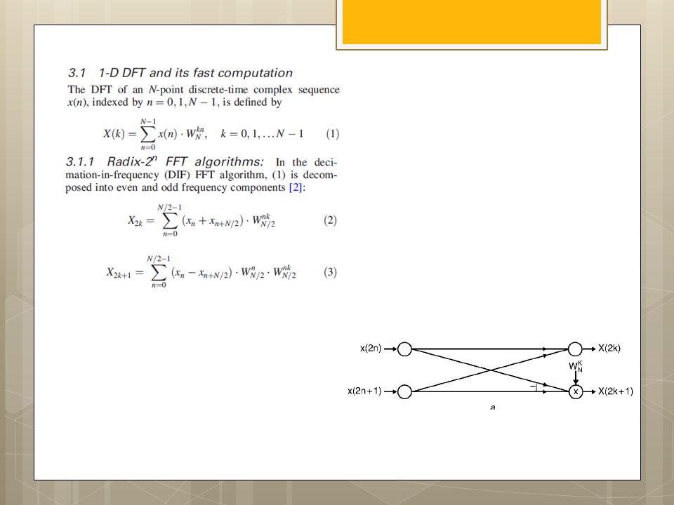
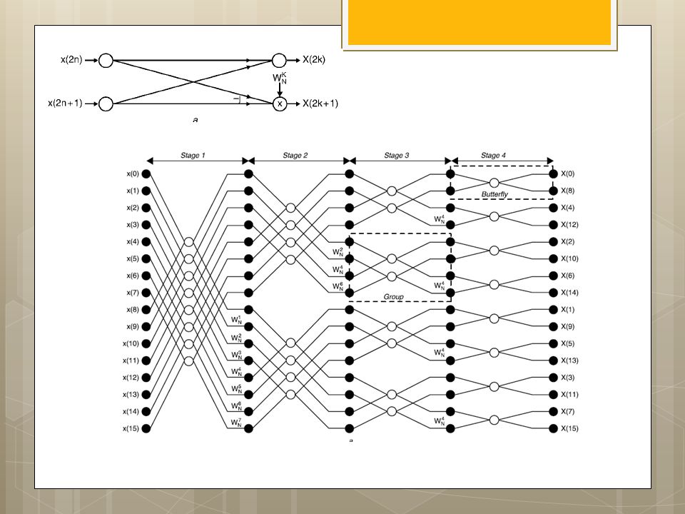
I.S. Uzun, A. Amira and A. Bouridane
FPGA implementations of fast Fourier transforms for real-time signal & image processing I.S. Uzun, A. Amira and A. Bouridane

40
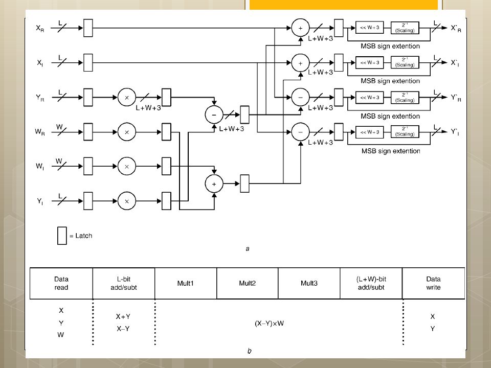
Functional block diagram of 1-D FFT processor architecture

43
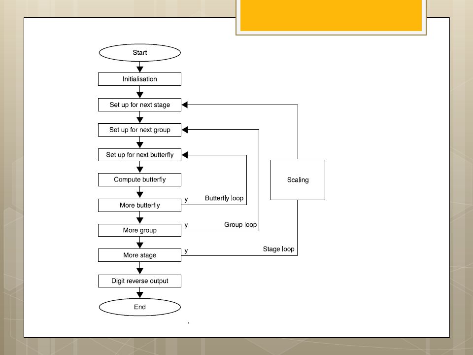
AGU: Radix-2 DIF FFT w s :¼ 1 for stage :¼ log 2 ðNÞ to
1 step 1 fnnstage loop m :¼ 2^stage is :¼ m=2 w index0 :¼ 0 for group :¼ 0 to n m step m fnngroup loop for bfi :¼ 0 to is l fnnbutterfly loop Index0 :¼ r þ j IEE Proc.-Vis. Image Signal Process., Vol. 152, No. 3, June Index1 :¼ Index0 þ is; } w index0 :¼ w index0 þ w s; w s :¼ w s 1 FIX THIS COPY WRONG

49
Hidden Slides

50
Number Representation
Fixed Point Floating-point Lower cost and higher speed. Added design effort for algorithm implementation analysis, and data and coefficient scaling to avoid accumulator overflow. Large dynamic range – range limitations can be ignored in a design. No need for scaling Flexibility More expensive – implement more functionality (complexity) in silicon and have wider buses. Appropriate in systems where gain coefficients change with time, or coefficients with large dynamic ranges. Deciding whether fixed or floating piont is more appropriate for the problem must be done carefully, preferably at an early phase in the project. In general, it can be assumed that fixed-point implementations have higher speed and lower cost, while floating-point has higherdynamic range and no need for scaling, which m Fixed point represent and manipulate numbers as integers Floating point processors represent numbers in floating point format can also support integer representation and calculations. Numerical value representation is a combination of mantissa (fractional part) and an exponent. Algorithms designed for fixed point Applications for Mobile TV. Bulk of signal chain processing is in the standard decoders, like MPEG-2, MPEG-4, JPEG-2000 and H.264. Greater precision and dynamic range are not helpful because algorithms are bit exact. V.g. Transform to go to frequency domain in video codecs ias some form of a DCT (Discrete Cosine Transform). DCT in video codecs are designed to br performed on a fixed-point processor and are bit exact. Unsigned Signed-Magnitude MSB is sign. Advantage: simplified prevention of overflows Disadvantage: addition must be split depending on which operand is larger. Two’s Complement (2C) Most popular signed number system in DSP use today. Possible to add several N-size signed numbers ; as long as the final sum is in the N-bit range, we can ignore any overflow in arithmetic. One’s Complement (1C) Needs a “carry wrap-around” addition; MSB must be added to LSB to get final correct result. Efficient to implement module 2N- --special value for DSP algorithms like Mersenne transforms. Diminished One System (D1) Has a bias of 1 compared to 2C A complement and add of the inverted carry must be computed. Used to implement Fermat NTTs. Bias System Has a bias for all numbers; for addition the bias needs to be substracted; for substraction added. Used to simplify comparison of numbers – coding the exponent of floating point numbers Signed Digit Numbers {0, 1, -1} Useful in carry-free adders or multipliers with less complexity (like Multiplier Adder Graph) Non-unique representation. Cost of multiplication is a direct function of number of nozero elements. Canonic Signed Digit System – CSD – system with min. number of non-zero elements. Optimal CSD – min. number of nonzero terms, but also min. number of substractions. Implementation of adder:- 28x4 –bit Lut Logarithmic Number System (LNS) Efficiently implement multiplication, division, square-rooting, or squaring. Add and substraction are more complex. Residue Numeral System Ancient algebraic system. Use small RAM or ROM tables to implement the modular mapings. For small wordl engths, RNS provide a significant speed-up using the 24x2 bit tables of Xilinx XC4000 FPGA. Altera FLEX allows larger moduli with the 28x8-bit table. Effort in multiplication can be estimated through the number of nonzero elements, which can be reduced by using SD numbers. Statistically, half the digits in a two’s compemetn coding are zer . For SD code, density of zeros increases to 2/3. Algorithm: starting ith the LSB substitue all 1 sequences equal or larger two, with 10…01 Breaking up an number into exponent and mantissa requires pre- and post-processing Some operations are easier than others Multiplication requires the addition of exponents, but mantissas are multiplied as though they were integers Addition requires barrel shifters to align inputs such that the mantissas are added when exponents are equal Handle corner cases +/- Infinity NaN (not-a-number) Denormalized numbers (exponent = 0)
 in silicon and have wider buses. Appropriate in systems where gain coefficients change with time, or coefficients with large dynamic ranges. Deciding whether fixed or floating piont is more appropriate for the problem must be done carefully, preferably at an early phase in the project. In general, it can be assumed that fixed-point implementations have higher speed and lower cost, while floating-point has higherdynamic range and no need for scaling, which m. Fixed point represent and manipulate numbers as integers. Floating point processors represent numbers in floating point format. can also support integer representation and calculations. Numerical value representation is a combination of mantissa (fractional part) and an exponent. Algorithms designed for fixed point. Applications for Mobile TV. Bulk of signal chain processing is in the standard decoders, like MPEG-2, MPEG-4, JPEG-2000 and H.264. Greater precision and dynamic range are not helpful because algorithms are bit exact. V.g. Transform to go to frequency domain in video codecs ias some form of a DCT (Discrete Cosine Transform). DCT in video codecs are designed to br performed on a fixed-point processor and are bit exact. Unsigned. Signed-Magnitude. MSB is sign. Advantage: simplified prevention of overflows. Disadvantage: addition must be split depending on which operand is larger. Two’s Complement (2C) Most popular signed number system in DSP use today. Possible to add several N-size signed numbers ; as long as the final sum is in the N-bit range, we can ignore any overflow in arithmetic. One’s Complement (1C) Needs a carry wrap-around addition; MSB must be added to LSB to get final correct result. Efficient to implement module 2N- --special value for DSP algorithms like Mersenne transforms. Diminished One System (D1) Has a bias of 1 compared to 2C. A complement and add of the inverted carry must be computed. Used to implement Fermat NTTs. Bias System. Has a bias for all numbers; for addition the bias needs to be substracted; for substraction added. Used to simplify comparison of numbers – coding the exponent of floating point numbers. Signed Digit Numbers {0, 1, -1} Useful in carry-free adders or multipliers with less complexity (like Multiplier Adder Graph) Non-unique representation. Cost of multiplication is a direct function of number of nozero elements. Canonic Signed Digit System – CSD – system with min. number of non-zero elements. Optimal CSD – min. number of nonzero terms, but also min. number of substractions. Implementation of adder:- 28x4 –bit Lut. Logarithmic Number System (LNS) Efficiently implement multiplication, division, square-rooting, or squaring. Add and substraction are more complex. Residue Numeral System. Ancient algebraic system. Use small RAM or ROM tables to implement the modular mapings. For small wordl engths, RNS provide a significant speed-up using the 24x2 bit tables of Xilinx XC4000 FPGA. Altera FLEX allows larger moduli with the 28x8-bit table. Effort in multiplication can be estimated through the number of nonzero elements, which can be reduced by using SD numbers. Statistically, half the digits in a two’s compemetn coding are zer . For SD code, density of zeros increases to 2/3. Algorithm: starting ith the LSB substitue all 1 sequences equal or larger two, with 10…01. Breaking up an number into exponent and mantissa requires pre- and post-processing. Some operations are easier than others. Multiplication requires the addition of exponents, but mantissas are multiplied as though they were integers. Addition requires barrel shifters to align inputs such that the mantissas are added when exponents are equal. Handle corner cases. +/- Infinity. NaN (not-a-number) Denormalized numbers (exponent = 0)")
51
Mapping Multithreaded Kernels
The simplest way of mapping functions to FPGA is to replicate hardware for each thread – inefficient and wasteful. Better methods involve taking advantage of pipeline parallelism Attempt to create a deeply pipelined representation of a kernel On each clock cycle, attempt to send in input data for a new thread Method of mapping coarse grained thread parallelism to fine-grained FPGA parallelism.

52
Example Pipeline for Vector Add
On each cycle the portions of the pipeline are processing different threads. Whiel thread 2 is being loaded, thread 1 is being added, and thread 0 is being stored.

53
Computer Arithmetic Careful choice of the bit width in FPGA design can result in substantial savings. Survey of number representations FPGAs allow a wide variety o computer arithmetic icimpleentations for the desired DSP alogrithm , because of the physical bit-level programming architecture. This constrasts with the programmable digital signal processors (PDSPs) with the fixed multiply accumulator core. Careful choice of the bit width in FPGA design can result in substantial savings. Number representations (fixed-point, floating-point) Basic operations ( + , X ) More difficult operations (square roots, trig. Functions) FIXED POINT AND FLOATING POINT HAVE: 1. Different internal implementation 2. Instruction sets 3. Algorithm implementation approaches
 with the fixed multiply accumulator core. Careful choice of the bit width in FPGA design can result in substantial savings. Number representations (fixed-point, floating-point) Basic operations ( + , X ) More difficult operations (square roots, trig. Functions) FIXED POINT AND FLOATING POINT HAVE: 1. Different internal implementation. 2. Instruction sets. 3. Algorithm implementation approaches.")
54
Document Filtering More examples: Raw performance metric of FFT reported in billion floating point operations per second (Gflop/s) calculated as 1/runtime scaled by a constant that is the standard nominal operation count. Bandwith efficiency = performance normalized to available memory bandwith (Gflop/s)/(Gbyte/s), Power efficiency = performance normalized to power consumed (Gflops/s)/Watt.
 calculated as 1/runtime scaled by a constant that is the standard nominal operation count. Bandwith efficiency = performance normalized to available memory bandwith (Gflop/s)/(Gbyte/s), Power efficiency = performance normalized to power consumed (Gflops/s)/Watt.")
55
Why FPGAs for DSP? A high number of NAND gates is needed to build a simple DSP object. A fast 4-bit adder, for example, uses about 130 NAND gates. On FPGA Can use slower clock and still get better throughput. Since frequency is lower can get lower power application too. Food for thought: A fast 4-bit adder uses about 130 NAND gates. *Gallagher, Sean. Mapping DSP Algorithms into FPGAs

56
Multiplier configurations
Variable Precision DSP Blocks in Stratix V Devices

57
Multiplier configurations
SP Blocks in Stratix & Stratix GX Devices (2005)
")
58
Modern FPGA families Fast carry logic FPGA + DSP Processor
Consolidation of Glue logic Memory Interfaces ASSP Delays (less than 0.5 ns per bit) Fast adders with large bit width No need for expensive “carry look-ahead” decoders. Modern FPGA families provide the best DSP complexity and maximum speed. This is attributed to the fact that modern devices provide fast-carry logic (sect ,p16) with delays (less than 0.5 ns per bit) that allow fast adders with large bit width, without the need for expensive “carry look-ahead” decoders. FPGA + DSP FPGA enables DSP processor acceleration – mapping speed critical loop of DSP code to FPGA. FPGA also enable consolidation of glue logic, memory, interfaces, ASSP -> RESEARCH WHAT IS ASSP!
 Fast adders with large bit width. No need for expensive carry look-ahead decoders. Modern FPGA families provide the best DSP complexity and maximum speed. This is attributed to the fact that modern devices provide fast-carry logic (sect ,p16) with delays (less than 0.5 ns per bit) that allow fast adders with large bit width, without the need for expensive carry look-ahead decoders. FPGA + DSP. FPGA enables DSP processor acceleration – mapping speed critical loop of DSP code to FPGA. FPGA also enable consolidation of glue logic, memory, interfaces, ASSP -> RESEARCH WHAT IS ASSP!")
Similar presentations


 Dr. Konstantinos Tatas.>")


 – –a fixed array of AND gates.>")
>")


 Architecture and Modeling (A paper review) Jason Luu ECE University of Toronto Oct 27, 2009.>")


 ◦ Spatially distributed sensors to monitor physical or environmental conditions, and to cooperatively.>")

 Digital Filters Digital filters are rapidly replacing classic analog.>")