Download presentation
Presentation is loading. Please wait.

1
Transmitter for Quantum Encryption System Supervisor: Yossi Hipsh Performed by: Asaf Holzer Edward Shifman High Speed Digital Systems Laboratory Final presentation Spring 2006

2
Background Several methods can be used for encrypting information. One of them is the BB84 scheme, which was developed by Brassard & Bennett. The advantage of this method is that it is impossible to crack it, because it is based on the “No Cloning” principle. The BB84 scheme was mathematically proved as a perfectly safe Method, in a theoretical perfect world without noises.

3
Project Objectives The transmitter module is part of a complex system, which purpose is to send a digital code, which will later be used as key for encrypting and decrypting information. Our goal is to produce an electrical pulse which is ~0.5ns wide and its magnitude is 4v. The purpose of this pulse is to activate the laser diode.

4
The Overall System Block Diagram Computer + Labview TransmitterReciever Interferometers, etc. Computer + Counter Synchronization

5
Original Plan Pulse trigger D.D.LTTL 2 ECL ECL Programmable Delay Chip 1:2 ECL Programmable Delay Chip Long fiber And Gate1:2 Bal_UN Gain P_QuantP_Sync monostable

6
Original Plan – continued… Pulse trigger D.D.LTTL 2 ECL ECL Programmable Delay Chip 1:2 ECL Programmable Delay Chip Long fiber And Gate1:2 Bal_UN Gain RefP_Stab monostable

7
In order to improve the module’s performance we decided to use ECL technology from the very beginning of the pulse module, so we put the TTL-ECL device at the beginning. We replaced the components so they will operate in 3.3 voltage level. Some more advances

8
Pulse trigger TTL 2 ECL ECL Prog. Delay Chip 1:2And Gate 1:4 Bal_UN Gain monostable ECL Prog. Delay Chip ECL Prog. Delay Chip … … … P_Quant P_Sync Ref Plan #2

9
Plan #3 Computer – LabView 1:4 (TTL) Mux TTL-ECL Pulse-Module 1:4 (TTL) sel counter P_QuantP_StabP_Sync stab_ensync_ctrltrig detector ref
 Mux TTL-ECL Pulse-Module 1:4 (TTL) sel counter P_QuantP_StabP_Sync stab_ensync_ctrltrig detector ref")
10
The Monostable (ECL) – Take #1… Flip Flop S R Q D ECL Prog. Delay Chip 1 ECL Prog. Delay Chip 3 ECL Prog. Delay Chip 2 1:4 (ECL) Q CLK MC100EP31 MC100EP31 Characteristics:
 Q CLK MC100EP31 MC100EP31 Characteristics:.")
11
The Monostable Timing Diagram Data CLK Reset Q tsts t clk-Q t R-Q Q 400ps130ps Min. Pulse width: 530ps t t t t

12
Plan #3 – Pulse Module monostable And Gate 1:2 Bal_UN Gain Plan B 3ns0.5ns 10ns ref

13
Flip Flop S R Q D ECL Prog. Delay Chip 2 ECL Prog. Delay Chip 1 1:4 (ECL) Q CLK Plan #3 – Pulse Module Flip Flop S R Q D ECL Prog. Delay Chip 3 ECL Prog. Delay Chip 5 ECL Prog. Delay Chip 4 1:4 (ECL) Q CLK 3ns 0.5ns And Gate 0.5ns
 Q CLK Plan #3 – Pulse Module Flip Flop S R Q D ECL Prog. Delay Chip 3 ECL Prog. Delay Chip 5 ECL Prog. Delay Chip 4 1:4 (ECL) Q CLK 3ns 0.5ns And Gate 0.5ns.")
14
Voltage Surfaces Vcc - 3.3V Vtt – 1.3V GND We ended up with one voltage source of 3.3V. Using a regulator to get 1.3V and a DC/DC converter to get 5V.

15
Voltage Surfaces

16
The Original Bal-UN IN OUT 68Ω 140Ω 150Ω 1nF 100nF + - V tt =1.3v

17
The Final Bal-UN IN OUT 68Ω 140Ω + - V tt =1.3v

18
The Final ORCAD Design

20
The Final ORCAD Design: Pulse-Module:

21
The Final ORCAD Design Test Points: Counter_tp – The detector has detected p_quan. Splitter14_tp – A pulse trigger has been received. Quan_tp Stab_tp Sync_tp Testing each Pulse Module

22
Connectors Power Connector SMA Connector Flat-Cable Connector

23
The Final Layout

24
Component List ComponentDescriptionManufacturerQuantity NB3L553_D1:4 TTLON Semi1 MC100EP11_DT1:2 PECLON Semi6 SN74F74_NFF (monostable)TI2 MC100EPT20_DTTTL to PECLON Semi3 MC100EPT21_DTPECL to TTLON Semi1 MC100EP58_DTMultiplexerON Semi1 MC100EP195_FAECL Prog. DelayON Semi9 SN7LVC1G125_DCKEnable BufferTI1 MC100EP05_DTAND GateON Semi3 PTH04000WAH_EUSRegulatorTI1 DC/DC Step-Up ConverterDC/DC ConverterTekgear1 ZPUL-30PAmplifierMini Circuits6

25
Power & Connectors List ComponentDescriptionManufacturerQuantity HWS10-3/APower SupplierLambda1 SMA8410L-9000SMA ConnectorJYEBAO12 CTB9300/6APower ConnectorCamden1 17978-150Flat ConnectorFCI1

26
PART B

27
Stack & Lines Design: Raw material used – Fr 4 W = 7mil Calculated using Microstrip equations, to achieve

28
Stack & Lines Design: Raw material used – Fr 4 W = 7mil Calculated using Stripline equations, to achieve

29
Stack & Lines Design:

30
HyperLynx Simulation First Assuming

31
HyperLynx Simulation Simulation Results for various frequencies @500MHz@2000MHz

32
HyperLynx Simulation Falling Edge Simulation

33
HyperLynx Simulation Simulation Results for various frequencies @500MHz@2000MHz Now Assuming Delay =

34
HyperLynx Simulation Simulation until now using S – distance between the lines Field Influence @ S=8mil Field Influence @ S=20mil

35
HyperLynx Simulation - Vias HyperLynx does not support Vias, so we had to model the via, using a capacitor & a resistor.

36
HyperLynx Simulation - Vias Simulation results for various frequencies @500MHz @1000MHz

37
HyperLynx Simulation - Vias Running a simulation without modeling the vias (with same total length of the transmission line) @500MHz @1000MHz

38
HyperLynx Simulation - Conclusion Impedance Coordination & Reflections Delays Crosstalk Via’s influence

39
The FPGA Field ProgrammableGateArray

40
FPGA Design Opcode structure: Mode (1bit)Pulse_editmode (2bit)Pulse_width (10bit)Pulse_offset (11bit) Mode (1bit) Pulse_workmode (3bit) Edit Mode: Work Mode: 0 1
Pulse_editmode (2bit)Pulse_width (10bit)Pulse_offset (11bit) Mode (1bit) Pulse_workmode (3bit) Edit Mode: Work Mode: 0 1")
41
CommentNameSize(bit) Field 0 – Edit mode 1 – Work mode Mode1 Opcode(23) Chosen Pulse modulePulse_editmode2Opcode(22-21) [500ps.. 4000ps]Pulse_width10Opcode(20-11) [4500ps.. 18500ps]Pulse_offset11Opcode(10-0) Chosen pulse-module/sPulse_workmode3Opcode(22-20) FPGA Design
 [4500ps ps]Pulse_offset11Opcode(10-0) Chosen pulse-module/sPulse_workmode3Opcode(22-20) FPGA Design.")
42
The FPGA – VHDL Design

44
Delay 1 Delay 2 Delay 3 LEN offset_temp <= pulse_offset - const_440; PROCESS(clk) BEGIN if (offset_temp(10) = '1') then first_offset <= const_1023; second_offset <= offset_temp(9 downto 0) + "0000000001"; else first_offset <= offset_temp(9 downto 0); second_offset <= const_0; end if; END PROCESS; delay1 <= first_offset; delay2 <= second_offset; delay3 <= second_offset +const_450- pulse_width; Delay Decode
 BEGIN if (offset_temp(10) = 1 ) then first_offset <= const_1023; second_offset <= offset_temp(9 downto 0) ; else first_offset <= offset_temp(9 downto 0); second_offset <= const_0; end if; END PROCESS; delay1 <= first_offset; delay2 <= second_offset; delay3 <= second_offset +const_450- pulse_width; Delay Decode")
45
The FPGA – Delay Set:

46
The FPGA – TESTBENCH:

48
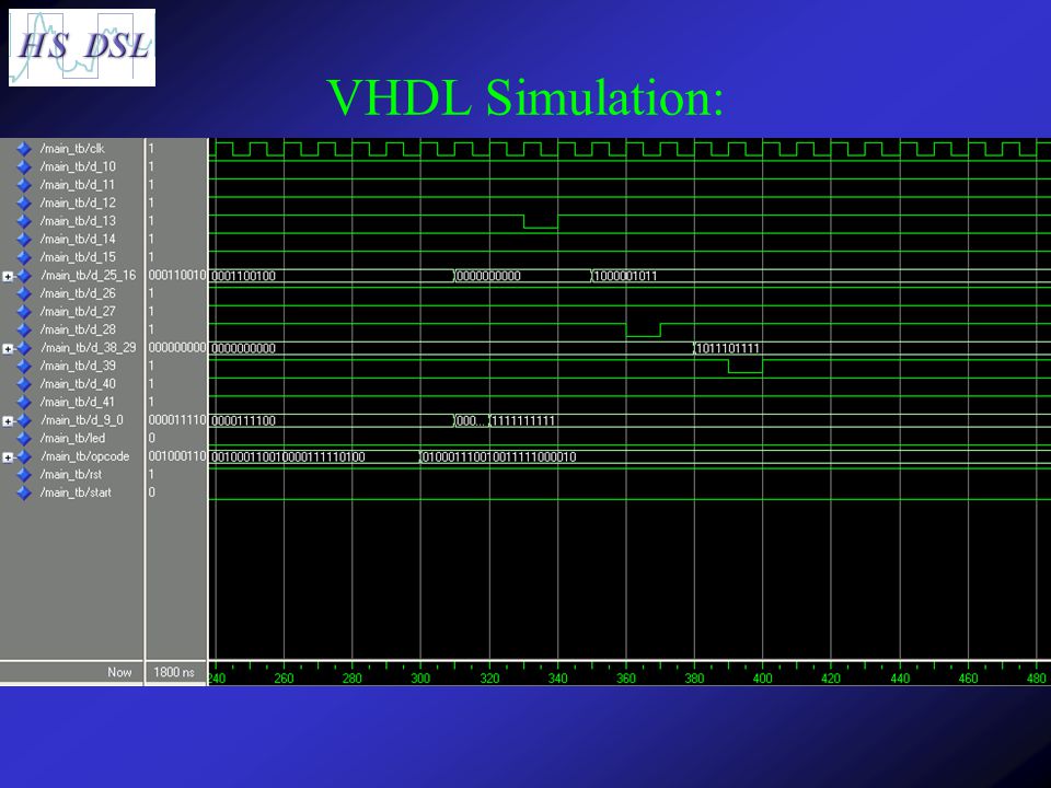
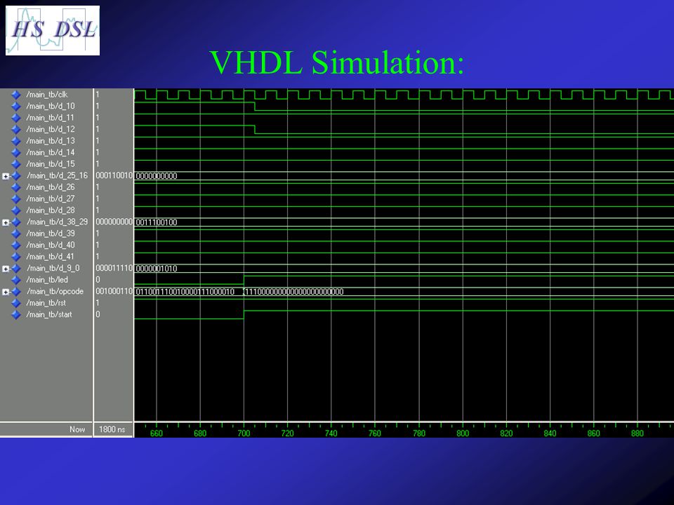
VHDL Simulation:

51
Supplemental Value: The project gave us experience in performing a large scale product, which involves several development groups, and provided us systemic vision. In the process of developing the project we enriched ourselves with techniques of high-speed systems and high- frequency phenomena. We experienced working with design & simulation tools such as: ORCAD, HDL Designer and HyperLynx. One of the most valuable principles we’ve learned is board design.

52
Future possibilities: The elementary step now would be sending our design to printing and testing it when it’s ready. In order to make the product user-friendly, we would have now built a graphical interface which translates the desired pulses shapes to appropriate sets of opcodes. The opcodes should be sent to the FPGA via USB connection.

53
Supplemental Value: The project gave us experience in performing a large scale product, which involves several development groups, and provided us systemic vision. In the process of developing the project we enriched ourselves with techniques of high-speed systems and high- frequency phenomena. We experienced working with design & simulation tools such as: ORCAD, HDL Designer and HyperLynx. One of the most valuable principles we’ve learned is board design.

Similar presentations


>")


 Instructor: Yossi Hipsh Students: Lior Shkolnitsky, Yevgeniy.>")


