Download presentation
Presentation is loading. Please wait.

1
D0525 Project Receiver for Quantum Encryption System By: Dattner Yony & Sulkin Alex Supervisor: Yossi Hipsh High Speed Digital Systems Laboratory Spring 2006

2
Introduction & Motivation 1.Due to the latest massive growth of computer networks, in military and public, and government institutes there arises a vital need for I.S.S (Information Secured systems) 2. Quantum encryption using the BB84 protocol has been mathematically proven to be 100% secure in an ideal world without noise. This is mainly due to the uncertainty principle regarding photons.

3
So far 1. We finished new design with improvements to the old design. 2. All the major components have been chosen. 3. Block Modules finished. 4. Orcad design for blocks has begun.

4
Improvements to the old design 1. We got rid of the monostable from the design which in turn simplifies the circuit. 2. We got rid of the mixer which causes old design to be less effective and efficient. 3. We use mostly only ecl components which allows a much faster design. 4. Two simple pulse modules for all the design.

5
The receiver design

6
No mixer policy As u saw we got rid of the mixer from the old design. The mixer caused us unnecessary transfers from balanced to unbalanced and caused us to leave the pure ecl pathway for the fast pulse. We wanted to stay with a balanced ecl technology for the fast pulse all the way till the gieger pulse interaction. Our solution is to amplify the gieger signal from 0.1 Volt to a high voltage and to delicately compare it with a reference voltage. Our delicate comparator will have ecl outputs so that now we can use an AND component with the fast pulse and the gieger signal which are now both balanced ecl signals. This solution allows us to stay on a balanced ecl pathway all the way till the end of the receiver.

7
Pulse module_2 for 260 ps block

8
1:2 DDL 3 ns 260 ps Tr=Tf=130 ps AND 130 ps 3 ns

9
Inputs and Outputs with the system Receiver sync and_select_1and_select_2 From_geiger_1 From_geiger_2 Count_1 Count_2 To_geiger_1 To_geiger_2 sync_1 sync_2 Control FPGA

10
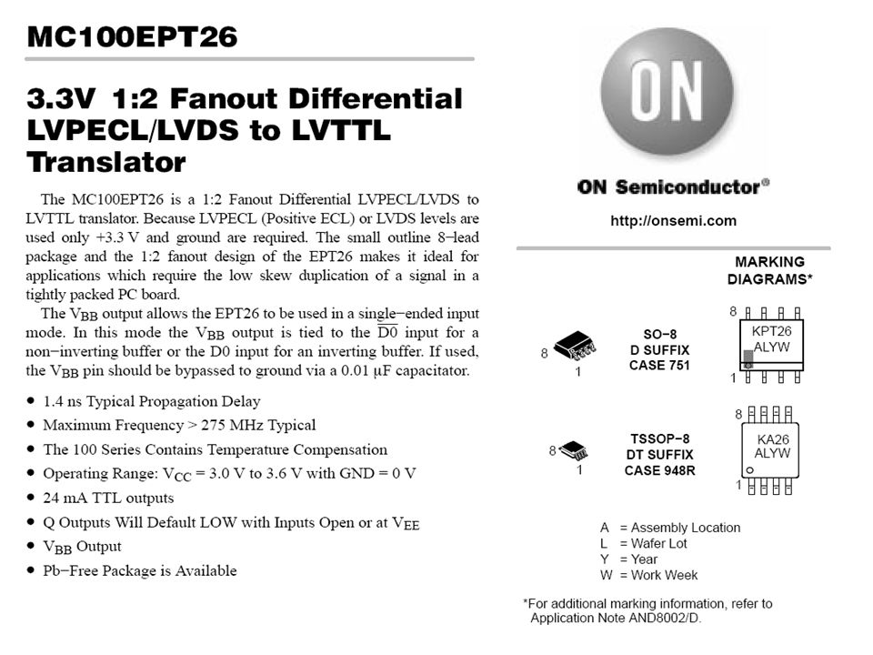
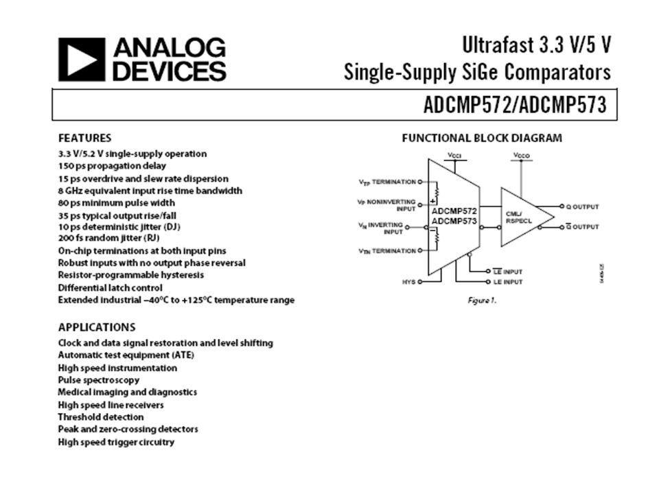
Part List

21
Buff 1:3 Block

22
ECL DDL Block.

23
Stretcher Block.

24
Future Plans. 1. Finish the final planning of all the components and to finish the electrical schematic of the design (orcad). 2. Making sure that all our components have been ordered supplied. 3. Deciding between wire up board or soldered board. 4. To plan and arrange the components position on the board and to plan the box for the design. 5. Designing and writing the logic controls for the project as well as the FPGA. 6. To physically build the project. 7. To design the tests for the project and to test the project to see that it works. 8. Write the final report of the working project and to get a grade.
. 2. Making sure that all our components have been ordered supplied. 3. Deciding between wire up board or soldered board. 4. To plan and arrange the components position on the board and to plan the box for the design. 5. Designing and writing the logic controls for the project as well as the FPGA. 6. To physically build the project. 7. To design the tests for the project and to test the project to see that it works. 8. Write the final report of the working project and to get a grade..")
Similar presentations


 - Ed Jastrzembski.>")


 Winter-Spring 2006.>")


