Download presentation
Presentation is loading. Please wait.

0
Princess Sumaya University
Digital Logic Design Digital Logic Design Chapter 4: Combinational Logic Dr. Bassam Kahhaleh

1
Combinational Circuits
Output is function of input only i.e. no feedback When input changes, output may change (after a delay) Combinational Circuits n inputs m outputs • •
 Combinational. Circuits. n inputs. m outputs. • • ")
2
Combinational Circuits
Analysis Given a circuit, find out its function Function may be expressed as: Boolean function Truth table Design Given a desired function, determine its circuit ? ?

3
(A’+B’)(A’+C’)(B’+C’)
Analysis Procedure Boolean Expression Approach ABC A+B+C AB'C'+A'BC'+A'B'C (A’+B’)(A’+C’)(B’+C’) AB+AC+BC F1=AB'C'+A'BC'+A'B'C+ABC F2=AB+AC+BC
(A’+C’)(B’+C’) AB+AC+BC. F1=AB C +A BC +A B C+ABC. F2=AB+AC+BC.")
4
Analysis Procedure Truth Table Approach A B C F1 F2 = 0 1

5
Analysis Procedure Truth Table Approach A B C F1 F2 0 0 0 0 0 1 1 0
= 0 = 1 1 1 1 1

6
Analysis Procedure Truth Table Approach A B C F1 F2 0 0 0 0 0 1 1
1 = 0 = 1 1 1 1 1

7
Analysis Procedure Truth Table Approach A B C F1 F2 0 0 0 0 0 1 1
1 = 0 = 1 1 1

8
Analysis Procedure Truth Table Approach A B C F1 F2 0 0 0 0 0 1 1
1 = 1 = 0 1 1 1 1

9
Analysis Procedure Truth Table Approach A B C F1 F2 0 0 0 0 0 1 1
1 = 1 = 0 1 1

10
Analysis Procedure Truth Table Approach A B C F1 F2 0 0 0 0 0 1 1
1 = 1 = 0 1 1

11
Analysis Procedure Truth Table Approach F1=AB'C'+A'BC'+A'B'C+ABC
1 = 1 1 1 1 B 1 A C B 1 A C F1=AB'C'+A'BC'+A'B'C+ABC F2=AB+AC+BC

12
? Design Procedure Given a problem statement: Example:
Determine the number of inputs and outputs Derive the truth table Simplify the Boolean expression for each output Produce the required circuit Example: Design a circuit to convert a “BCD” code to “Excess 3” code ? 4-bits 0-9 values 4-bits Value+3

13
BCD-to-Excess 3 Converter
Design Procedure BCD-to-Excess 3 Converter C 1 B A x D C 1 B A x D A B C D w x y z x x x x w = A+BC+BD x = B’C+B’D+BC’D’ C 1 B A x D C 1 B A x D y = C’D’+CD z = D’

14
BCD-to-Excess 3 Converter
Design Procedure BCD-to-Excess 3 Converter A B C D w x y z x x x x w = A + B(C+D) y = (C+D)’ + CD x = B’(C+D) + B(C+D)’ z = D’
 y = (C+D)’ + CD. x = B’(C+D) + B(C+D)’ z = D’")
15
Seven-Segment Decoder
a b c g e d f w x y z a b c d e f g x x x x x x x ? w x y z a b c d e f g BCD code y 1 x w z a = w + y + xz + x’z’ b = . . . c = . . . d = . . .

16
Binary Adder Half Adder Adds 1-bit plus 1-bit Produces Sum and Carry
x y S C x + y ─── C S x y C S 0 0 0 0 0 1 0 1 1 0 1 1 1 0 x y S C

17
Binary Adder Full Adder Adds 1-bit plus 1-bit plus 1-bit
Produces Sum and Carry FA x y z S C x + y + z ─── C S y 1 x z x y z C S 0 0 0 1 1 0 1 1 S = xy'z'+x'yz'+x'y'z+xyz = x y z y 1 x z C = xy + xz + yz

18
Binary Adder Full Adder x S S y x y C z z C
S = xy'z'+x'yz'+x'y'z+xyz = x y z C = xy + xz + yz x y z S C S C x y z

19
Binary Adder Full Adder HA HA x y z S C x y z S C

20
Carry Propagate Addition
Binary Adder Binary Adder x3x2x1x y3y2y1y0 S3S2S1S0 C0 Cy c3 c2 c + x3 x2 x1 x0 + y3 y2 y1 y0 ──────── Cy S3 S2 S1 S0 Carry Propagate Addition x x x x0 y y y y0 FA FA FA FA C C C C1 S S S S0

21
Binary Adder Carry Propagate Adder CPA CPA x7 x6 x5 x4 x3 x2 x1 x0
y7 y6 y5 y4 y3 y2 y1 y0 CPA A3 A2 A1 A0 B3 B2 B1 B0 S3 S2 S1 S0 C0 Cy CPA A3 A2 A1 A0 B3 B2 B1 B0 Cy C0 S3 S2 S1 S0 S7 S6 S5 S4 S3 S2 S1 S0

22
Operands and Result: 0 to 9
BCD Adder 4-bits plus 4-bits Operands and Result: 0 to 9 + x3 x2 x1 x0 + y3 y2 y1 y0 ──────── Cy S3 S2 S1 S0 X +Y x3 x2 x1 x0 y3 y2 y1 y0 Sum Cy S3 S2 S1 S0 0 + 0 = 0 0 + 1 = 1 0 + 2 = 2 0 + 9 = 9 1 + 0 = 1 1 + 1 = 2 1 + 8 = 9 1 + 9 = A Invalid Code 2 + 0 = 2 9 + 9 = 12 1 Wrong BCD Value

23
BCD Adder + 6 X +Y x3 x2 x1 x0 y3 y2 y1 y0 Sum Cy S3 S2 S1 S0
Required BCD Output Value 9 + 0 = 9 9 + 1 = 10 = 16 9 + 2 = 11 = 17 9 + 3 = 12 = 18 9 + 4 = 13 = 19 9 + 5 = 14 = 20 9 + 6 = 15 = 21 9 + 7 1 = 22 9 + 8 = 23 9 + 9 = 24 + 6

24
Correct Binary Adder’s Output (+6)
BCD Adder Correct Binary Adder’s Output (+6) If the result is between ‘A’ and ‘F’ If Cy = 1 S3 S2 S1 S0 Err 1 S1 S2 S3 1 S0 Err = S3 S2 + S3 S1
 If the result is between ‘A’ and ‘F’ If Cy = 1. S3 S2 S1 S0. Err S1. S2. S3. 1. S0. Err = S3 S2 + S3 S1.")
25
BCD Adder Err

26
Use 2’s complement with binary adder
Binary Subtractor Use 2’s complement with binary adder x – y = x + (-y) = x + y’ + 1
 = x + y’ + 1.")
27
Binary Adder/Subtractor
M: Control Signal (Mode) M=0 F = x + y M=1 F = x – y
 M=0 F = x + y. M=1 F = x – y.")
28
Unsigned Binary Numbers
Overflow Unsigned Binary Numbers 2’s Complement Numbers FA x x x x0 y y y y0 S S S S0 C C C C1 Carry FA x x x x0 y y y y0 S S S S0 C C C C1 Overflow

29
Compare 4-bit number to 4-bit number
Magnitude Comparator Compare 4-bit number to 4-bit number 3 Outputs: < , = , > Expandable to more number of bits A3A2A1A0 B3B2B1B0 Magnitude Comparator A<B A=B A>B

30
Magnitude Comparator

31
Magnitude Comparator Magnitude Comparator Magnitude Comparator
x7 x6 x5 x4 x3 x2 x1 x0 y7 y6 y5 y4 y3 y2 y1 y0 Magnitude Comparator A3 A2 A1 A0 B3 B2 B1 B0 A<B A=B A>B I(A>B) I(A=B) I(A<B) Magnitude Comparator A3 A2 A1 A0 B3 B2 B1 B0 1 I(A>B) I(A=B) I(A<B) A<B A=B A>B A<B A=B A>B
 I(A=B) I(A<B) Magnitude Comparator. A3 A2 A1 A0. B3 B2 B1 B0. 1. I(A>B) I(A=B) I(A<B) A<B A=B A>B. A<B A=B A>B.")
32
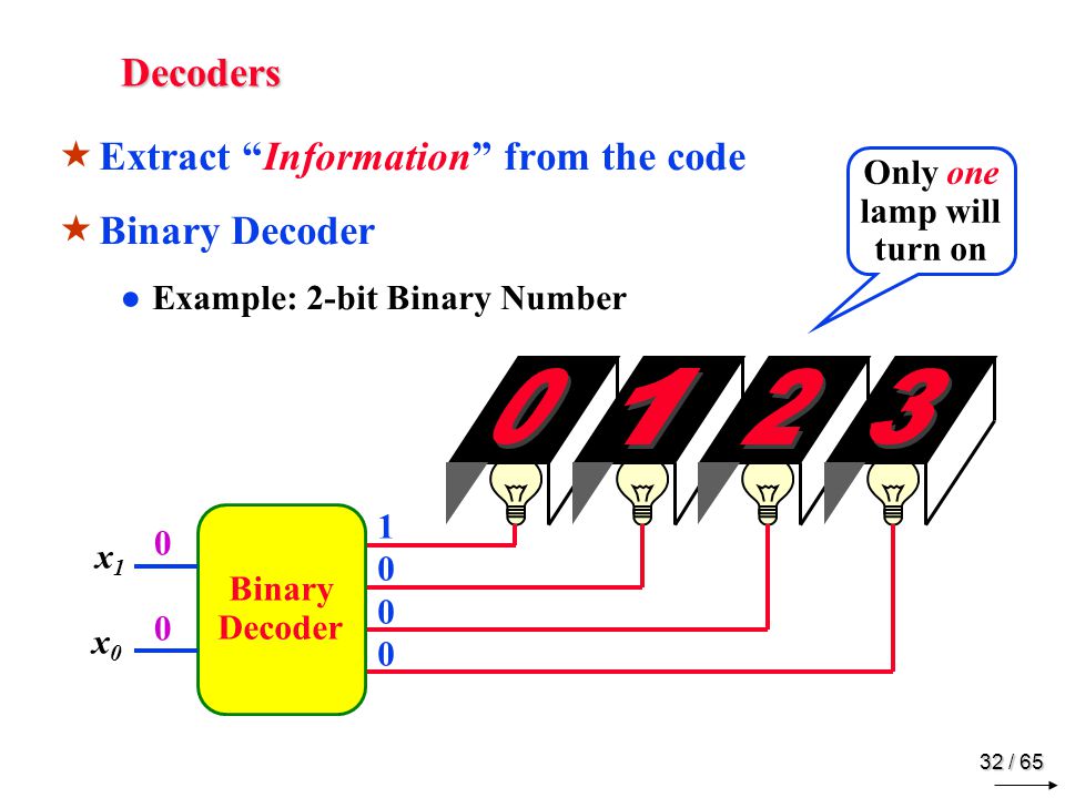
Only one lamp will turn on
Decoders Extract “Information” from the code Binary Decoder Example: 2-bit Binary Number Only one lamp will turn on 1 2 3 Binary Decoder x1 x0 1

33
Decoders 2-to-4 Line Decoder Binary Decoder I1 I0 y3 y2 y1 y0 I1 I0
0 0 0 1 1 0 1 1
34
Decoders 3-to-8 Line Decoder Y7 Y6 Y5 Binary Decoder Y4 Y3 Y2 I2 Y1 I1

35
Decoders “Enable” Control Binary Decoder I1 I0 E Y3 Y2 Y1 Y0 E I1 I0
x x 1 0 0 0 1 1 0 1 1

36
Decoders Expansion I2 I1 I0 I2 I1 I0 Y7 Y6 Y5 Y4 Y3 Y2 Y1 Y0 0 0 0
Binary Decoder I0 I1 E Y3 Y2 Y1 Y0 Y7 Y6 Y5 Y4

37
Active-High / Active-Low
Decoders Active-High / Active-Low I1 I0 Y3 Y2 Y1 Y0 0 0 0 1 1 0 1 1 I1 I0 Y3 Y2 Y1 Y0 0 0 0 1 1 0 1 1 Binary Decoder I1 I0 Y3 Y2 Y1 Y0 Binary Decoder I1 I0 Y3 Y2 Y1 Y0

38
Implementation Using Decoders
Each output is a minterm All minterms are produced Sum the required minterms Example: Full Adder S(x, y, z) = ∑(1, 2, 4, 7) C(x, y, z) = ∑(3, 5, 6, 7) I2 I1 I0 Y7 Y6 Y5 Y4 Y3 Y2 Y1 Y0 Binary Decoder x y z S C
 = ∑(1, 2, 4, 7) C(x, y, z) = ∑(3, 5, 6, 7) I2. I1. I0. Y7. Y6. Y5. Y4 Y3. Y2. Y1. Y0. Binary Decoder. x. y. z. S C.")
39
Implementation Using Decoders
Y7 Y6 Y5 Y4 Y3 Y2 Y1 Y0 Binary Decoder x y z S C I2 I1 I0 Y7 Y6 Y5 Y4 Y3 Y2 Y1 Y0 Binary Decoder x y z S C

40
Only one switch should be activated at a time
Encoders Put “Information” into code Binary Encoder Example: 4-to-2 Binary Encoder Only one switch should be activated at a time 1 2 3 Binary Encoder y1 y0 x1 x2 x3 x3 x2 x1 y1 y0 0 0 0 1 1 0 1 1

41
Octal-to-Binary Encoder (8-to-3)
Encoders Octal-to-Binary Encoder (8-to-3) Binary Encoder Y2 Y1 Y0 I7 I6 I5 I4 I3 I2 I1 I0 I7 I6 I5 I4 I3 I2 I1 I0 Y2 Y1 Y0
 Binary Encoder. Y2. Y1. Y0. I7. I6. I5. I4 I3. I2. I1. I0. I7 I6 I5 I4 I3 I2 I1 I0. Y2 Y1 Y")
42
4-Input Priority Encoder
Priority Encoders 4-Input Priority Encoder Priority Encoder V Y1 Y0 I3 I2 I1 I0 I3 I2 I1 I0 Y1 Y0 V 0 0 1 x 0 1 x x 1 0 1 x x x 1 1 Y1 I1 1 I2 I3 I0

43
Encoder / Decoder Pairs
Binary Encoder Binary Decoder Y7 Y6 Y5 Y4 Y3 Y2 Y1 Y0 7 7 I7 I6 I5 I4 I3 I2 I1 I0 6 6 5 5 Y2 Y1 Y0 I2 I1 I0 4 4 3 3 2 2 1 1

44
Multiplexers S1 S0 Y 0 0 I0 0 1 I1 1 0 I2 1 1 I3 MUX Y I0 I1 I2 I3
0 0 I0 0 1 I1 1 0 I2 1 1 I3 MUX Y I0 I1 I2 I3 S1 S0

45
Multiplexers 2-to-1 MUX 4-to-1 MUX I0 MUX I1 Y S I0 I1 MUX I2 I3 Y
S1 S0

46
Multiplexers Quad 2-to-1 MUX x3 y3 x2 y2 x1 y1 x0 y0 I0 MUX I1 Y S S
S E Y3 Y2 Y1 Y0 B3 B2 B1 B0 S

47
Multiplexers Quad 2-to-1 MUX A3 A2 A1 A0 MUX Y3 Y2 Y1 Y0 B3 B2 B1 B0
S E Y3 Y2 Y1 Y0 B3 B2 B1 B0 Extra Buffers

48
Implementation Using Multiplexers
Example F(x, y) = ∑(0, 1, 3) x y F 0 0 1 0 1 1 0 1 1 MUX Y I0 I1 I2 I3 S1 S0 1 F x y
 = ∑(0, 1, 3) x y. F MUX. Y. I0. I1. I2. I3. S1 S0. 1. F. x y.")
49
Implementation Using Multiplexers
Example F(x, y, z) = ∑(1, 2, 6, 7) MUX Y I0 I1 I2 I3 I4 I5 I6 I7 S2 S1 S0 1 x y z F 1 F x y z
 = ∑(1, 2, 6, 7) MUX. Y. I0. I1. I2. I3 I4. I5. I6. I7. S2 S1 S0. 1. x y z. F F. x y z.")
50
Implementation Using Multiplexers
Example F(x, y, z) = ∑(1, 2, 6, 7) x y z F 1 MUX Y I0 I1 I2 I3 S1 S0 z F = z F z F = z 1 F = 0 x y F = 1
 = ∑(1, 2, 6, 7) x y z. F MUX. Y. I0. I1. I2. I3. S1 S0. z. F = z. F. z. F = z. 1. F = 0. x y. F = 1.")
51
Implementation Using Multiplexers
Example F(A, B, C, D) = ∑(1, 3, 4, 11, 12, 13, 14, 15) A B C D F 1 MUX Y I0 I1 I2 I3 I4 I5 I6 I7 S2 S1 S0 D F = D D F = D D F = D F F = 0 D F = 0 1 F = D 1 F = 1 F = 1 A B C
 = ∑(1, 3, 4, 11, 12, 13, 14, 15) A B C D. F MUX. Y. I0. I1. I2. I3 I4. I5. I6. I7. S2 S1 S0. D. F = D. D. F = D. D. F = D. F. F = 0. D. F = F = D. 1. F = 1. F = 1. A B C.")
52
Multiplexer Expansion
8-to-1 MUX using Dual 4-to-1 MUX Y I0 I1 I2 I3 I4 I5 I6 I7 S2 S1 S0 MUX Y I0 I1 I2 I3 S1 S0 MUX Y I0 I1 S MUX Y I0 I1 I2 I3 S1 S0 1 0 0

53
DeMultiplexers DeMUX I Y3 Y2 Y1 Y0 S1 S0 S1 S0 Y3 Y2 Y1 Y0 0 0 I 0 1
0 0 I 0 1 1 0 1 1

54
Multiplexer / DeMultiplexer Pairs
MUX DeMUX Y7 Y6 Y5 Y4 Y3 Y2 Y1 Y0 7 7 I7 I6 I5 I4 I3 I2 I1 I0 6 6 5 5 4 4 Y I 3 3 2 2 1 1 S2 S1 S0 S2 S1 S0 Synchronize x2 x1 x0 y2 y1 y0

55
DeMultiplexers / Decoders
DeMUX I Y3 Y2 Y1 Y0 S1 S0 Binary Decoder I1 I0 E Y3 Y2 Y1 Y0 E I1 I0 Y3 Y2 Y1 Y0 x x 1 0 0 0 1 1 0 1 1 S1 S0 Y3 Y2 Y1 Y0 0 0 I 0 1 1 0 1 1

56
Three-State Gates Tri-State Buffer Tri-State Inverter C A Y 0 x Hi-Z
1 0 1 1 1 A Y C A Y C

57
Three-State Gates C D Y 0 0 Hi-Z 0 1 B 1 0 A 1 1 ? A Y C B Not Allowed
0 0 Hi-Z 0 1 B 1 0 A 1 1 ? A Y C B Not Allowed D A C B A if C = 1 B if C = 0 Y=

58
Three-State Gates I3 I2 Y I1 I0 Y3 Binary Decoder Y2 S1 I1 Y1 I0 Y0 E

59
Homework Mano Chapter 4 4-2 4-3 4-5 4-11 4-13 4-27 4-28 4-31 4-32 4-33
4-35

60
Homework Mano 4-2 Obtain the simplified Boolean expressions for output F and G in terms of the input variables in the circuit:

61
Homework 4-3 For the circuit shown in the “Quad 2-to-1 MUX”:
(a) Write the Boolean functions for the four outputs in terms of the input variables (b) If the circuit is listed in a truth table, how many rows and columns would there be in the truth table? 4-5 Design a combinational circuit with three inputs, x, y, and z, and three outputs, A, B, and C. When the binary input is 0, 1, 2, or 3, the binary output is one greater than the input. When the binary input is 4, 5, 6, or 7, the binary output is one less than the input.
 Write the Boolean functions for the four outputs in terms of the input variables. (b) If the circuit is listed in a truth table, how many rows and columns would there be in the truth table 4-5. Design a combinational circuit with three inputs, x, y, and z, and three outputs, A, B, and C. When the binary input is 0, 1, 2, or 3, the binary output is one greater than the input. When the binary input is 4, 5, 6, or 7, the binary output is one less than the input.")
62
Homework 4-11 Design a 4-bit combinational circuit incrementer. (A circuit that adds one to a 4-bit binary number.) The circuit can be designed using four half-adders. 4-13 The adder-subtractor circuit has the following values for mode input M and data inputs A and B. In each case, determine the values of the four SUM outputs and the carry C. M A B (a) (b) (c) (d) (e)
 The circuit can be designed using four half-adders The adder-subtractor circuit has the following values for mode input M and data inputs A and B. In each case, determine the values of the four SUM outputs and the carry C. M A B. (a) (b) (c) (d) (e)")
63
Homework 4-27 A combinational circuit is specified by the following three Boolean functions: F1(A, B, C) = ∑(2, 4, 7) F2(A, B, C) = ∑(0, 3) F3(A, B, C) = ∑(0, 2, 3, 4, 7) Implement the circuit with a decoder constructed with NAND gates and NAND or AND gates connected to the decoder outputs. Use a block diagram for the decoder. Minimize the number of inputs in the external gates.
 = ∑(0, 3) F3(A, B, C) = ∑(0, 2, 3, 4, 7) Implement the circuit with a decoder constructed with NAND gates and NAND or AND gates connected to the decoder outputs. Use a block diagram for the decoder. Minimize the number of inputs in the external gates.")
64
Homework 4-28 A combinational circuit is defined by the following three Boolean functions: F1 = x’ y’ z’ + x z F2 = x y’ z’ + x’ y F3 = x’ y’ z + x y Design the circuit with a decoder and external gates. 4-31 Construct a 16 1 multiplexer with two 8 1 and one 2 1 multiplexers. Use block diagrams. 4-32 Implement the following Boolean function with a multiplexer: F(A, B, C, D) = ∑(0, 1, 3, 4, 8, 9, 15)
 = ∑(0, 1, 3, 4, 8, 9, 15)")
65
Homework 4-33 Implement a full adder with two 4 1 multiplexers: 4-35
Implement the following Boolean function with a 4 1 multiplexer and external gates. Connect inputs A and B to the selection lines. The input requirements for the four data lines will be a function of variables C and D. These values are obtained by expressing F as a function of C and D for each of the four cases when AB = 00, 01, 10, and 11. These functions may have to be implemented with external gates. F(A, B, C, D) = ∑(1, 3, 4, 11, 12, 13, 14, 15)
 = ∑(1, 3, 4, 11, 12, 13, 14, 15)")
Similar presentations

>")
 Half-adder adds rightmost (least significant) bit Full-adder.>")


>")