Download presentation
Presentation is loading. Please wait.

1
Microprocessor System Design

2
Outline Address decoding Chip select Memory configurations

3
Minimum Mode When Memory is selected?

4
Minimum Mode 2 20 bytes or 1MB

5
What are the memory locations of a 1MB (2 20 bytes) Memory? A19 to A0 (HEX) AAAA 1111 9876 AAAA 1111 5432 AAAA 1198 1000 AAAA 7654 AAAA 3210 000000000 FFFFF1111 Example: 34FD0 0011 0100 11111 1101 0000
 AAAA AAAA AAAA AAAA 7654 AAAA FFFFF1111 Example: 34FD")
6
Interfacing a 1MB Memory to the 8088 Microprocessor

7
Instead of Interfacing 1MB, what will happen if you interface a 512KB Memory?

8
What are the memory locations of a 512KB (2 19 bytes) Memory? A18 to A0 (HEX) AAAA 1111 9876 AAAA 1111 5432 AAAA 1198 1000 AAAA 7654 AAAA 3210 000000000 7FFFF01111111
 AAAA AAAA AAAA AAAA 7654 AAAA FFFF")
9
Interfacing a 512KB Memory to the 8088 Microprocessor What do we do with A19?

10
What if you want to read physical address A0023?

11
A19 to A0 (HEX) AAAA 1111 9876 AAAA 1111 5432 AAAA 1198 1000 AAAA 7654 AAAA 3210 A002310100000 00100011 A19 is not connected to the memory so even if the 8088 microprocessor outputs a logic “1”, the memory cannot “see” this.
 AAAA AAAA AAAA AAAA 7654 AAAA 3210 A A19 is not connected to the memory so even if the 8088 microprocessor outputs a logic 1 , the memory cannot see this.")
12
What if you want to read physical address 20023? A18 to A0 (HEX) AAAA 1111 9876 AAAA 1111 5432 AAAA 1198 1000 AAAA 7654 AAAA 3210 2002300100000 00100011 For memory it is the same as previous one.
 AAAA AAAA AAAA AAAA 7654 AAAA For memory it is the same as previous one..")
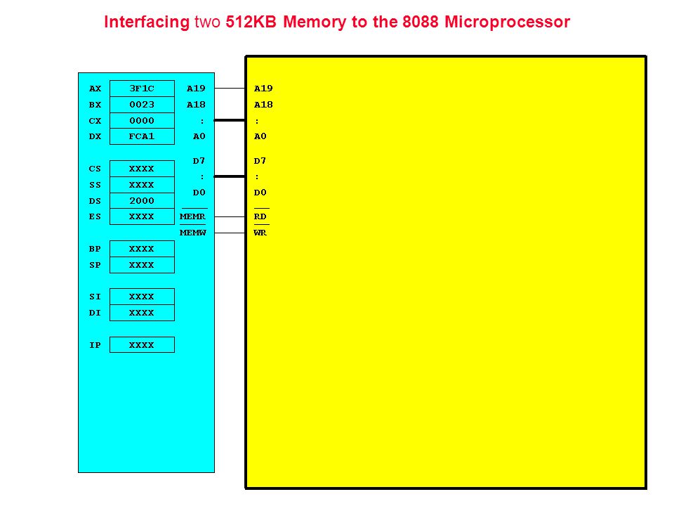
13
Interfacing two 512KB Memory to the 8088 Microprocessor

14
Problem: Bus Conflict. The two memory chips will provide data at the same time when microprocessor performs a memory read. Solution: Use address line A19 as an “arbiter”. If A19 outputs a logic “1” the upper memory is enabled (and the lower memory is disabled) and vice-versa.
 and vice-versa..")
15
Interfacing two 512KB Memory to the 8088 Microprocessor : RD WR CS

16
What are the memory locations of two consecutive 512KB (2 19 bytes) Memory? A19 to A0 (HEX) AAAA 1111 9876 AAAA 1111 5432 AAAA 1198 1000 AAAA 7654 AAAA 3210 000000000 7FFFF01111111 8000010000000 FFFFF1111
 AAAA AAAA AAAA AAAA 7654 AAAA FFFF FFFFF1111.")
17
Interfacing two 512KB Memory to the 8088 Microprocessor When the P outputs an address between 80000 to FFFFF, this memory is selected When the P outputs an address between 00000 to 7FFFF, this memory is selected

18
Interfacing two 512KB Memory to the 8088 Microprocessor

20
What if we remove the lower memory?

21
When the P outputs an address between 80000 to FFFFF, this memory is selected When the P outputs an address between 00000 to 7FFFF, no memory chip is selected !

22
Full and Partial Decoding Full Decoding –When all of the “useful” address lines are connected the memory/device to perform selection Partial Decoding –When some of the “useful” address lines are connected the memory/device to perform selection –Using this type of decoding results into roll-over addresses

23
Full Decoding

24
A19 to A0 (HEX) AAAA 1111 9876 AAAA 1111 5432 AAAA 1198 1000 AAAA 7654 AAAA 3210 8000010000000 FFFFF1111 A19 should be a logic “1” for the memory chip to be enabled
 AAAA AAAA AAAA AAAA 7654 AAAA FFFFF1111 A19 should be a logic 1 for the memory chip to be enabled")
25
Full Decoding A19 to A0 (HEX) AAAA 1111 9876 AAAA 1111 5432 AAAA 1198 1000 AAAA 7654 AAAA 3210 000000000 7FFFF01111111 Therefore if the microprocessor outputs an address between 00000 to 7FFFF, whose A19 is a logic “0”, the memory chip will not be selected
 AAAA AAAA AAAA AAAA 7654 AAAA FFFF Therefore if the microprocessor outputs an address between to 7FFFF, whose A19 is a logic 0 , the memory chip will not be selected")
26
Partial Decoding

27
A19 to A0 (HEX) AAAA 1111 9876 AAAA 1111 5432 AAAA 1198 1000 AAAA 7654 AAAA 3210 000000000 7FFFF01111111 8000010000000 FFFFF1111 The value of A19 is INSIGNIFICANT to the memory chip, therefore A19 has no bearing whether the memory chip will be enabled or not
 AAAA AAAA AAAA AAAA 7654 AAAA FFFF FFFFF1111 The value of A19 is INSIGNIFICANT to the memory chip, therefore A19 has no bearing whether the memory chip will be enabled or not")
28
Partial Decoding A19 to A0 (HEX) AAAA 1111 9876 AAAA 1111 5432 AAAA 1198 1000 AAAA 7654 AAAA 3210 000000000 7FFFF01111111 8000010000000 FFFFF1111 ACTUAL ADDRESS
 AAAA AAAA AAAA AAAA 7654 AAAA FFFF FFFFF1111 ACTUAL ADDRESS")
29
Partial Decoding A19 to A0 (HEX) AAAA 1111 9876 AAAA 1111 5432 AAAA 1198 1000 AAAA 7654 AAAA 3210 000000000 7FFFF01111111 8000010000000 FFFFF1111 ACTUAL ADDRESS
 AAAA AAAA AAAA AAAA 7654 AAAA FFFF FFFFF1111 ACTUAL ADDRESS")
30
Interfacing two 512K Memory Chips to the 8088 Microprocessor

31
Interfacing one 512K Memory Chips to the 8088 Microprocessor

32
Interfacing one 512K Memory Chips to the 8088 Microprocessor (version 2)
")
33
Interfacing one 512K Memory Chips to the 8088 Microprocessor (version 3)
")
34
Interfacing four 256K Memory Chips to the 8088 Microprocessor

36
Memory chip#__ is mapped to: A19 to A0 (HEX) AAAA 1111 9876 AAAA 1111 5432 AAAA 1198 1000 AAAA 7654 AAAA 3210 ----- ---- ---------
 AAAA AAAA AAAA AAAA 7654 AAAA")
37
Interfacing four 256K Memory Chips to the 8088 Microprocessor

40
Interfacing several 8K Memory Chips to the 8088 P

41
Interfacing 128 8K Memory Chips to the 8088 P

43
Memory chip#__ is mapped to: A19 to A0 (HEX) AAAA 1111 9876 AAAA 1111 5432 AAAA 1198 1000 AAAA 7654 AAAA 3210 ----- ---- ---------
 AAAA AAAA AAAA AAAA 7654 AAAA")
44
Memory Terms Capacity –Kbit, Mbit, Gbit Organization –Address lines –Data lines Speed / Timing –Access time Write ability –ROM –RAM

45
ROM Variations Mask Rom PROM – OTP EPROM – UV_EPROM EEPROM Flash memory

46
RAM Variations SRAM DRAM NV-RAM –SRAM – CMOS –Internal lithium battery –Control circuitry to monitor Vcc

47
Memory Chip 8K SRAM to be specific: –8Kx8 bits SRAM

48
6264 Block Diagram

49
6264 Function Table

50
Memory Chip 8K EPROM to be specific: –8Kx8 bits EPROM

51
2764 Block Diagram Chip enable Output enable

52
Operating Modes

53
Programming 2764 after each erasure for UV-EPROM): –all bits of the M2764A are in the “1" state. The only way to change a “0" to a ”1" is by ultraviolet light erasure. Programming mode when: –VPP input is at 12.5V –E and P are at TTL low. The data to the data output pins. The levels required for the address and data inputs are TTL.

54
Interfacing 128 8K Memory Chips to the 8088 P

Similar presentations


 access to programmable input/ output devices. It has three.>")


>")


