Download presentation
Presentation is loading. Please wait.

1
Lecture 10 Xilinx FPGA Memories Part 1
ECE 448 – FPGA and ASIC Design with VHDL

2
ECE 448 – FPGA and ASIC Design with VHDL
Recommended reading Spartan-6 FPGA Block RAM Resources: User Guide Google search: UG383 Spartan-6 FPGA Configurable Logic Block: User Guide Google search: UG384 Xilinx FPGA Embedded Memory Advantages: White Paper Google search: WP360 ISE In-Depth Tutorial, Section: Creating a CORE Generator Tool Module Google search: ISE In-Depth Tutorial ECE 448 – FPGA and ASIC Design with VHDL

3
Memory Types

4
Memory Types Memory Memory Memory RAM ROM Single port Dual port
With asynchronous read With synchronous read

5
Memory Types specific to Xilinx FPGAs
Distributed (MLUT-based) Block RAM-based (BRAM-based) Memory Inferred Instantiated Using CORE Generator Manually
 Block RAM-based (BRAM-based) Memory. Inferred. Instantiated. Using CORE Generator. Manually.")
6
FPGA Distributed Memory

7
Location of Distributed RAM
Logic resources (CLB slices) RAM blocks DSP units Logic resources (#Logic resources, #Multipliers/DSP units, #RAM_blocks) Graphics based on The Design Warrior’s Guide to FPGAs Devices, Tools, and Flows. ISBN Copyright © 2004 Mentor Graphics Corp. (
 RAM blocks. DSP units. Logic resources. (#Logic resources, #Multipliers/DSP units, #RAM_blocks) Graphics based on The Design Warrior’s Guide to FPGAs Devices, Tools, and Flows. ISBN Copyright © 2004 Mentor Graphics Corp. (")
8
Three Different Types of Slices
50% 25% 25% ECE 448 – FPGA and ASIC Design with VHDL

9
Spartan-6 Multipurpose LUT (MLUT)
32-bit SR 64 x 1 RAM 64 x 1 ROM (logic) The Design Warrior’s Guide to FPGAs Devices, Tools, and Flows. ISBN Copyright © 2004 Mentor Graphics Corp. (
 The Design Warrior’s Guide to FPGAs Devices, Tools, and Flows. ISBN Copyright © 2004 Mentor Graphics Corp. (")
10
ECE 448 – FPGA and ASIC Design with VHDL
Single-port 64 x 1-bit RAM ECE 448 – FPGA and ASIC Design with VHDL

11
Memories Built of Neighboring MLUTs
Memories built of 2 MLUTs: Single-port 128 x 1-bit RAM: RAM128x1S Dual-port x 1-bit RAM : RAM64x1D Memories built of 4 MLUTs: Single-port 256 x 1-bit RAM: RAM256x1S Dual-port x 1-bit RAM: RAM128x1D Quad-port x 1-bit RAM: RAM64x1Q Simple-dual-port 64 x 3-bit RAM: RAM64x3SDP (one address for read, one address for write) ECE 448 – FPGA and ASIC Design with VHDL
 ECE 448 – FPGA and ASIC Design with VHDL.")
12
ECE 448 – FPGA and ASIC Design with VHDL
Dual-port 64 x 1 RAM Dual-port 64 x 1-bit RAM : 64x1D Single-port 128 x 1-bit RAM: x1S ECE 448 – FPGA and ASIC Design with VHDL

13
Total Size of Distributed RAM

14
FPGA Block RAM

15
(#Logic resources, #Multipliers/DSP units, #RAM_blocks)
Location of Block RAMs Logic resources (CLB slices) RAM blocks DSP units Logic resources (#Logic resources, #Multipliers/DSP units, #RAM_blocks) Graphics based on The Design Warrior’s Guide to FPGAs Devices, Tools, and Flows. ISBN Copyright © 2004 Mentor Graphics Corp. (
 RAM blocks. DSP units. Logic resources. (#Logic resources, #Multipliers/DSP units, #RAM_blocks) Graphics based on The Design Warrior’s Guide to FPGAs Devices, Tools, and Flows. ISBN Copyright © 2004 Mentor Graphics Corp. (")
16
Spartan-6 Block RAM Amounts

17
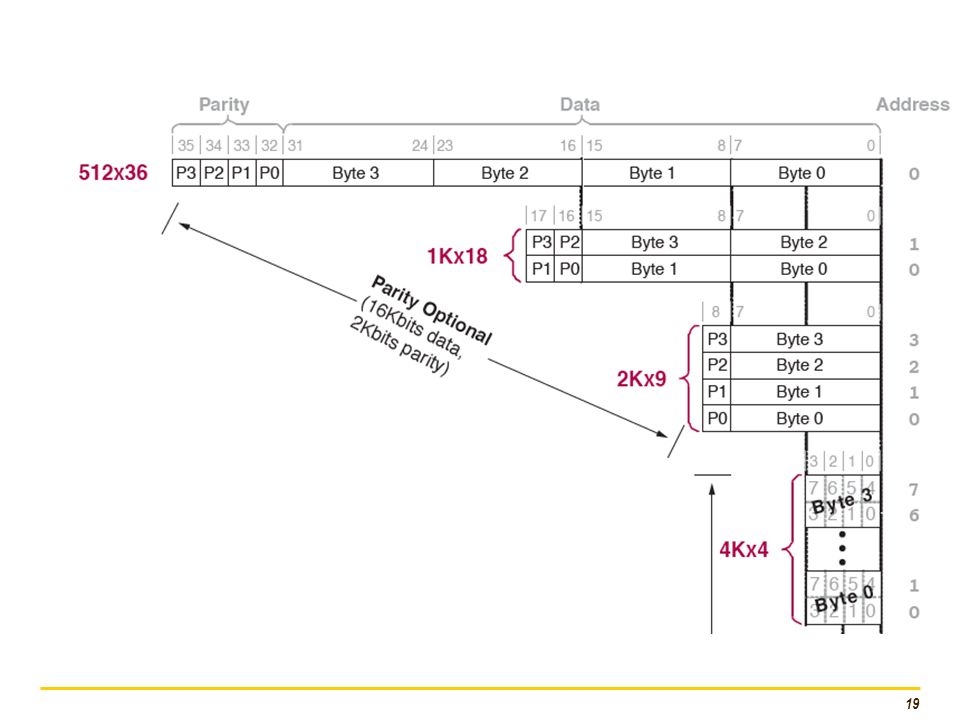
Block RAM can have various configurations (port aspect ratios)
1 2 4 4k x 4 8k x 2 4,095 16k x 1 8,191 8+1 2k x (8+1) 2047 16+2 1024 x (16+2) 1023 16,383
 x (16+2) ,383.")
20
Block RAM Port Aspect Ratios

21
Block RAM Interface

22
Block RAM Ports

23
Block RAM with synchronous read in Read-First Mode
CE

24
Features of Block RAMs in Spartan-6 FPGAs

Similar presentations


 COE 203 Digital Logic Laboratory Dr. Aiman El-Maleh College of Computer Sciences and Engineering.>")


