Download presentation
Presentation is loading. Please wait.

1
Xilinx CPLDs and FPGAs Module F2-1

2
CPLDs and FPGAs XC9500 CPLD XC4000 FPGA Spartan FPGA Spartan II FPGA Virtex FPGA

3
XC9500 CPLDs 5 volt in-system programmable (ISP) CPLDs 5 ns pin-to-pin 36 to 288 macrocells (6400 gates) Industry’s best pin- locking architecture 10,000 program/erase cycles Complete IEEE 1149.1 JTAG capability Function Block 1 JTAG Controller Function Block 2 I/O Function Block 4 3 Global Tri-States 2 or 4 Function Block 3 I/O In-System Programming Controller FastCONNECT Switch Matrix JTAG Port 3 I/O Global Set/Reset Global Clocks I/O Blocks 1
 CPLDs 5 ns pin-to-pin 36 to 288 macrocells (6400 gates) Industry’s best pin- locking architecture 10,000 program/erase cycles Complete IEEE JTAG capability Function Block 1 JTAG Controller Function Block 2 I/O Function Block 4 3 Global Tri-States 2 or 4 Function Block 3 I/O In-System Programming Controller FastCONNECT Switch Matrix JTAG Port 3 I/O Global Set/Reset Global Clocks I/O Blocks 1")
4
XC9500 Function Block To FastCONNECT From FastCONNECT 2 or 4 3 Global Tri-State Global Clocks I/O 36 Product- Term Allocator Macrocell 1 AND Array Macrocell 18 Each function block is like a 36V18 !

5
XC9500 Product Family 9536 Macrocells Usable Gates t PD (ns) Registers Max I/O 3672108144216 8001600240032004800 57.5 10 3672108144216 3472108133166 Packages VQ44 PC44 PC84 TQ100 PQ100 PC84 TQ100 PQ100 PQ160 PQ100 PQ160 288 6400 10 288 192 HQ208 BG352 PQ160 HQ208 BG352 957295108951449521695288
 Registers Max I/O Packages VQ44 PC44 PC84 TQ100 PQ100 PC84 TQ100 PQ100 PQ160 PQ100 PQ HQ208 BG352 PQ160 HQ208 BG")
6
CPLDs and FPGAs XC9500 CPLD XC4000 FPGA Spartan FPGA Spartan II FPGA Virtex FPGA

7
XC4000 Architecture Programmable Interconnect I/O Blocks (IOBs) Configurable Logic Blocks (CLBs)
 Configurable Logic Blocks (CLBs)")
8
XC4000E/X Configurable Logic Blocks 2 Four-input function generators (Look Up Tables) - 16x1 RAM or Logic function 2 Registers - Each can be configured as Flip Flop or Latch - Independent clock polarity - Synchronous and asynchronous Set/Reset
 - 16x1 RAM or Logic function 2 Registers - Each can be configured as Flip Flop or Latch - Independent clock polarity - Synchronous and asynchronous Set/Reset")
9
XC4000 CLB

10
Look Up Tables Capacity is limited by number of inputs, not complexity Choose to use each function generator as 4 input logic (LUT) or as high speed sync.dual port RAM Combinatorial Logic is stored in 16x1 SRAM Look Up Tables (LUTs) in a CLB Example: A B C D Z 0 0 0 0 0 0 0 0 1 0 0 0 1 0 0 0 0 1 1 1 0 1 0 0 1 0 1 0 1 1... 1 1 0 0 0 1 1 0 1 0 1 1 1 0 0 1 1 1 1 1 Look Up Table Combinatorial Logic A B C D Z 4-bit address G Func. Gen. G4 G3 G2 G1 WE 2 (2 ) 4 = 64K !
 4 = 64K !.")
11
XC4000X I/O Block Diagram Shaded areas are not included in XC4000E family.

12
Xilinx FPGA Routing 1) Fast Direct Interconnect - CLB to CLB 2) General Purpose Interconnect - Uses switch matrix CLB Switch Matrix Switch Matrix 3) Long Lines Segmented across chip Global clocks, lowest skew 2 Tri-states per CLB for busses Other routing types in CPLDs and XC6200
 Fast Direct Interconnect - CLB to CLB 2) General Purpose Interconnect - Uses switch matrix CLB Switch Matrix Switch Matrix 3) Long Lines Segmented across chip Global clocks, lowest skew 2 Tri-states per CLB for busses Other routing types in CPLDs and XC6200")
13
Other FPGA Resources Tri-state buffers for busses (BUFT’s) Global clock & high speed buffers (BUFG’s) Wide Decoders (DECODEx) Internal Oscillator (OSC4) Global Reset to all Flip-Flops, Latches (STARTUP) CLB special resources Fast Carry logic built into CLBs Synchronous Dual Port RAM Boundary Scan
 Global clock & high speed buffers (BUFG’s) Wide Decoders (DECODEx) Internal Oscillator (OSC4) Global Reset to all Flip-Flops, Latches (STARTUP) CLB special resources Fast Carry logic built into CLBs Synchronous Dual Port RAM Boundary Scan")
14
What’s Really In that Chip? CLB (Red) Switch Matrix Long Lines (Purple) Direct Interconnect (Green) Routed Wires (Blue) Programmable Interconnect Points, PIPs (White)
 Switch Matrix Long Lines (Purple) Direct Interconnect (Green) Routed Wires (Blue) Programmable Interconnect Points, PIPs (White).")
15
Xilinx XC4000E FPGAs

16
CPLDs and FPGAs XC9500 CPLD XC4000 FPGA Spartan FPGA Spartan II FPGA Virtex FPGA

17
Xilinx Spartan FPGAs

18
CPLDs and FPGAs XC9500 CPLD XC4000 FPGA Spartan FPGA Spartan II FPGA Virtex FPGA

20
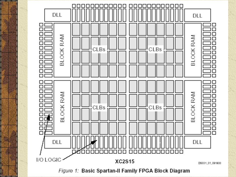
Xilinx Spartan-II FPGAs

21
Block RAM

23
Delay-Locked Loop

24
Phase-Locked Loop

25
CPLDs and FPGAs XC9500 CPLD XC4000 FPGA Spartan FPGA Spartan II FPGA Virtex FPGA

26
Virtex FPGAs

27
Virtex-II FPGAs

28
Virtex-II Pro FPGAs

Similar presentations


 –Up to 57 Kb block RAM storage Flexible.>")


 CPLDs 5 ns pin-to-pin 36 to 288 macrocells (6400 gates) Industry’s.>")


 Programmable.>")
