Download presentation
Presentation is loading. Please wait.

1
Honeywell Advanced Photonics Development Overview ATLAS Meeting January 7, 1999 John Lehman Honeywell Technology Center lehman_john@htc.honeywell.com www.htc.honeywell.com

2
Oxide VCSEL Development Status/Impact Low threshold/high slope efficiency demonstrated – Needed for low power operation/relaxes threshold/bias uniformity requirements High temperature operation demonstrated – Slope efficiency less temp. dependent than implants - less variation in output power – Required for military/rugged applications Uniformity demonstrated – Permits expansion to larger arrays (1D or 2D) Reliability demonstrated (preliminary) – Required Currently working to understand optimum device size for OMNET
 Reliability demonstrated (preliminary) – Required Currently working to understand optimum device size for OMNET.")
3
“Planar” Trench-Defined Oxide Structure Oxide layer exposed by etching trenches surrounding device Polymer Planarization not required Improved reliability/robustness Interconnect metal readily patterned More amenable to array fabrication

4
Honeywell Oxide VCSEL Reliability Over 240 oxide VCSELs samples A variety of temperatures and currents used to stress devices Preliminary data indicates oxide VCSEL reliability is equal to or better than implanted VCSELs (current Honeywell VCSEL MTTF > 10 7 hours at 40C 10mA) Oxide VCSELs show no degradation under 85%RH 85C exposure non-hermetic packaging
 Oxide VCSELs show no degradation under 85%RH 85C exposure non-hermetic packaging")
5
Exposures made at Phillips Laboratory NM. Honeywell Standard VCSEL Exposure to 4.5 MeV protons Total dose 1.51 x 10 14 p/cm 2 (119 Mrad total dose ; 4.9 x 10 10 ions/cm 2 /sec flux) Device recovers after 20mA constant current for 17 hrs. Post irradiation Pre-irradiation Post anneal Pre-irradiation VCSEL Demonstrates Operation in 119 Mrad Total Dose (4.5 MeV protons) Environment Baseline and Proton exposure L-I-V Baseline and post exposure anneal L-I-V
 Device recovers after 20mA constant current for 17 hrs. Post irradiation Pre-irradiation Post anneal Pre-irradiation VCSEL Demonstrates Operation in 119 Mrad Total Dose (4.5 MeV protons) Environment Baseline and Proton exposure L-I-V Baseline and post exposure anneal L-I-V.")
6
High speed properties of irradiated VCSEL Standard implanted VCSEL structure (850 nm) > 10 Mrad total dose (4.5 MeV protons) t r = 83 psec; t f = 104 psec
 > 10 Mrad total dose (4.5 MeV protons) t r = 83 psec; t f = 104 psec")
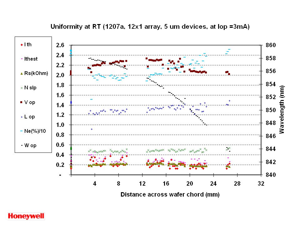
7
Uniformity & Yield of 3"-dia MOVPE-Grown Planar Oxide-Confined VCSEL Wafer HTC Wafer Growth/Process High Wafer Yield (99.7%est.) High Uniformity Utilizes In-House Commercially- Available MOVPE Chamber Material growth compatible with HI-Micro-Switch VCSEL Production
 High Uniformity Utilizes In-House Commercially- Available MOVPE Chamber Material growth compatible with HI-Micro-Switch VCSEL Production")
9
Next Generation VCSEL Array Uniformity Current (mA) Output Power (mW) Voltage (V) V op = 2 mA 12 channels 250 m pitch
 Output Power (mW) Voltage (V) V op = 2 mA 12 channels 250 m pitch")
10
Comparison COTS and ROV VCSEL Specs (Honeywell HFE4080-321 vs. Oxide typical 5um… Test conditions: 0C < T < 70C)
.")
11
Oxide VCSELs Demonstrating Range of High and Wide Temperature Operation

12
Threshold current temperature dependence - Oxide VCSEL 5 um diameter

13
Output Power (3mA) temperature dependence - Oxide VCSEL
 temperature dependence - Oxide VCSEL")
14
Comparison of Temperature performance - Oxide VCSEL/Implant

15
3mA - 30% 3mA + 30% 0.2mA + 30% 0.2mA - 30% Low Threshold VCSEL less sensitive to bias variations

16
Oxide Aperture size performance summary

17
Oxide VCSEL Aperture Size Dependent Parameters

18
Near Field and FF Photos of Oxide VCSELs 2.5um-dia SM Oxide9.5um-dia MM Oxide Near Field Far Field (HW)=13.5 0 (HW)=14.5 0
= (HW)=14.5 0")
19
Coupling vs Fiber Displacement

20
1Gb/s PRBS NRZ Eye diagram for Single-Mode oxide VCSEL: 1206bM2 2 m-dia; I th = 0.24mA; I hi = 3mA HP83487A head I l = 0 Gbit Ethernet RX: I l = IthGbit Ethernet RX: I l = 0 HP83487A head I l = Ith

21
Biased and Unbiased BER Characteristic for Single-Mode Oxide VCSEL: 1206b-G5-M2 (2- m dia): 1Gbit/s; I th = 0.24mA
: 1Gbit/s; I th = 0.24mA")
22
1Gb/s PRBS NRZ Eye diagram for MM Oxide VCSEL: 1206bM5 5 m-dia; I th = 0.38mA; I hi = 3mA HP83487A head I l = 0 HP83487A head I l = Ith Gbit Ethernet RX: I l = IthGbit Ethernet RX: I l = 0

23
Turn-on delay T d vs I hi for I L = 0; Multi-Mode Oxide VCSEL 1206b-M5: d= 5 m; I th = 0.38mA; l = 844nm

24
Biased and Unbiased BER Characteristic for Multi-Mode Oxide VCSEL: 1206b-G5-M5 (5- m dia): 1Gbit/s; I th = 0.38mA
: 1Gbit/s; I th = 0.38mA")
25
Pulse shape for Single-Mode oxide VCSEL: 2um-dia I th = 0.24mA; I hi = 3mA I l < I th I > I th I l =I th

26
Integrated MSM/MESFET Design – 6000 mV/mW – 120 m detector Hybrid CMOS TIA w/ GaAs PIN – 100 m diameter – t r,f < 50 psec – 0.64 A/W – <0.5 pF Receiver Approaches 400 Mb/s PRBS-7 12 channel receiver array

27
Transimpedance Amplifier Driving 50 /2pF Load for High Signal Input

28
Integrated MSM photodetector Typical device characteristics: Low dark current: Less than 10 nA @ 5V Responsivity: 0.34 (A/W) @ 5V for 850 nm wavelength Bandwidth: > 3 GHz MARKER ( 5.000 V9.713 nA ) OEP 903 100 um 2,3,4 150.0 u IF 20.0 u /div -150.0 u (A) o -10.0 VF (V) 2.00 /div 10.0 Typical MSM IV curves, Pin = 0.44 mW
 OEP um 2,3, u IF 20.0 u /div u (A) o VF (V) 2.00 /div 10.0 Typical MSM IV curves, Pin = 0.44 mW")
29
Clock sent on one fiber - 3 fibers/Mercury port (2.112 Gb/s data on 2 fibers, clk) 12 fibers for 4 ports MUX/DMUX, 8b/10b coding Open fiber control for eye safety I/O buffer specification RACEway Router RxB OMNET I/O 16 2 Data 1 Clk 12 VCSEL/Rx array 12 channel optical output(input) 16 Bits @132 Mb/s (electrical) 8B/10B 1.32 Gb/s (optical)
 12 fibers for 4 ports MUX/DMUX, 8b/10b coding Open fiber control for eye safety I/O buffer specification RACEway Router RxB OMNET I/O 16 2 Data 1 Clk 12 VCSEL/Rx array 12 channel optical output(input) 16 Mb/s (electrical) 8B/10B 1.32 Gb/s (optical)")
30
IBM 6SF CMOS Foundry Standard Features 0.25 m lithography 0.18 m L effective 2.5 V 4 level metal 200 mm wafer Epi on p bulk Single level poly Tungsten filled vias Options: diffused resistors, polysilicon/diffusion capacitor, metal to metal capacitors, polysilicon resistors, additional levels of metal

31
Architecture of the buffer

Similar presentations


>")
 Jin-Sung Youn>")

