Download presentation
Presentation is loading. Please wait.

1
Introduction to Computer Engineering CS/ECE 252, Spring 2012 Prof. Karu Sankaralingam Computer Sciences Department University of Wisconsin – Madison

2
Chapter 3 Digital Logic Structures Slides based on set prepared by Gregory T. Byrd, North Carolina State University

3
Copyright © The McGraw-Hill Companies, Inc. Permission required for reproduction or display. 3-3 Transistor: Building Block of Computers Show LED flashlight Battery, Switch, LED Normal state: Switch open, no current, no light Push botton: Switch closed, current flows, light

4
Copyright © The McGraw-Hill Companies, Inc. Permission required for reproduction or display. 3-4 Simple Switch Circuit Switch open: No current through circuit Light is off V out is +2.9V Switch closed: Short circuit across switch Current flows Light is on V out is 0V Switch-based circuits can easily represent two states: on/off, open/closed, voltage/no voltage.

5
Copyright © The McGraw-Hill Companies, Inc. Permission required for reproduction or display. 3-5 N-type MOS Transistor MOS = Metal Oxide Semiconductor two types: N-type and P-type N-type when Gate has positive voltage, short circuit between #1 and #2 (switch closed) when Gate has zero voltage, open circuit between #1 and #2 (switch open) Gate = 1 Gate = 0 Terminal #2 must be connected to GND (0V).
 when Gate has zero voltage, open circuit between #1 and #2 (switch open) Gate = 1 Gate = 0 Terminal #2 must be connected to GND (0V)..")
6
Copyright © The McGraw-Hill Companies, Inc. Permission required for reproduction or display. 3-6 P-type MOS Transistor P-type is complementary to N-type when Gate has positive voltage, open circuit between #1 and #2 (switch open) when Gate has zero voltage, short circuit between #1 and #2 (switch closed) Gate = 1 Gate = 0 Terminal #1 must be connected to +2.9V.
 when Gate has zero voltage, short circuit between #1 and #2 (switch closed) Gate = 1 Gate = 0 Terminal #1 must be connected to +2.9V..")
7
Copyright © The McGraw-Hill Companies, Inc. Permission required for reproduction or display. 3-7 Logic Gates Use switch behavior of MOS transistors to implement logical functions: AND, OR, NOT. Digital symbols: recall that we assign a range of analog voltages to each digital (logic) symbol assignment of voltage ranges depends on electrical properties of transistors being used typical values for "1": +5V, +3.3V, +2.9V, +1.1V for purposes of illustration, we'll use +2.9V
 symbol assignment of voltage ranges depends on electrical properties of transistors being used typical values for 1 : +5V, +3.3V, +2.9V, +1.1V for purposes of illustration, we ll use +2.9V.")
8
Copyright © The McGraw-Hill Companies, Inc. Permission required for reproduction or display. 3-8 CMOS Circuit Complementary MOS Uses both N-type and P-type MOS transistors P-type Attached to + voltage Pulls output voltage UP when input is zero N-type Attached to GND Pulls output voltage DOWN when input is one For all inputs, make sure that output is either connected to GND or to +, but not both! Draw generic CMOS gate w/ P and N blocks.

9
Copyright © The McGraw-Hill Companies, Inc. Permission required for reproduction or display. World’s first transistor (1947)
.")
10
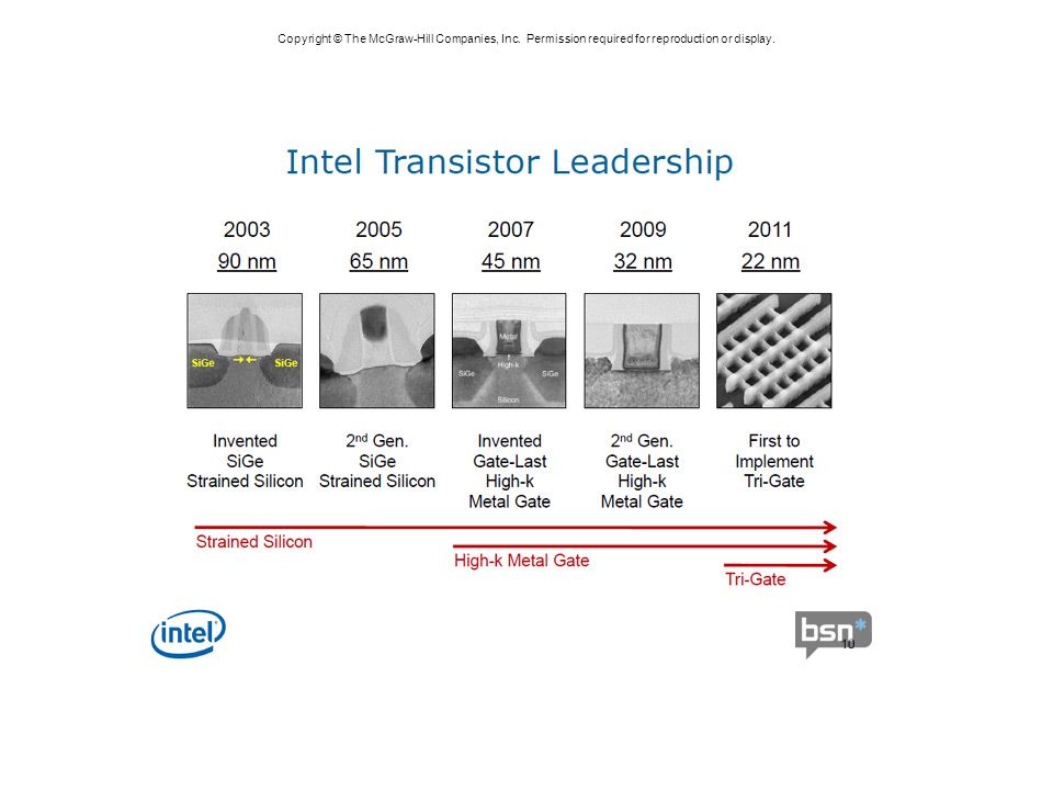
Copyright © The McGraw-Hill Companies, Inc. Permission required for reproduction or display.

12
Intel’s Tri-gate transistor

13
Copyright © The McGraw-Hill Companies, Inc. Permission required for reproduction or display. 3-13 Inverter (NOT Gate) InOut 0 V2.9 V 0 V InOut 01 10 Truth table
 InOut 0 V2.9 V 0 V InOut Truth table.")
14
Copyright © The McGraw-Hill Companies, Inc. Permission required for reproduction or display. 3-14 NOR Gate ABC 001 010 100 110 Note: Serial structure on top, parallel on bottom.

15
Copyright © The McGraw-Hill Companies, Inc. Permission required for reproduction or display. 3-15 OR Gate Add inverter to NOR. ABC 000 011 101 111

16
Copyright © The McGraw-Hill Companies, Inc. Permission required for reproduction or display. 3-16 NAND Gate (AND-NOT) ABC 001 011 101 110 Note: Parallel structure on top, serial on bottom.
 ABC Note: Parallel structure on top, serial on bottom..")
17
Copyright © The McGraw-Hill Companies, Inc. Permission required for reproduction or display. 3-17 AND Gate Add inverter to NAND. ABC 000 010 100 111

18
Copyright © The McGraw-Hill Companies, Inc. Permission required for reproduction or display. 3-18 Basic Logic Gates

19
Copyright © The McGraw-Hill Companies, Inc. Permission required for reproduction or display. 3-19 More than 2 Inputs? AND/OR can take any number of inputs. AND = 1 if all inputs are 1. OR = 1 if any input is 1. Similar for NAND/NOR. Can implement with multiple two-input gates, or with single CMOS circuit.

20
Copyright © The McGraw-Hill Companies, Inc. Permission required for reproduction or display. 3-20 Practice Implement a 3-input NOR gate with CMOS.

21
Copyright © The McGraw-Hill Companies, Inc. Permission required for reproduction or display. 3-21 Logical Completeness Can implement ANY truth table with AND, OR, NOT. ABCD 0000 0010 0101 0110 1000 1011 1100 1110 1. AND combinations that yield a "1" in the truth table. 2. OR the results of the AND gates.

22
Copyright © The McGraw-Hill Companies, Inc. Permission required for reproduction or display. 3-22 Practice Implement the following truth table. ABC 000 011 101 110

23
Copyright © The McGraw-Hill Companies, Inc. Permission required for reproduction or display. 3-23 DeMorgan's Law Converting AND to OR (with some help from NOT) Consider the following gate: AB 001110 011001 100101 110001 Same as A+B! To convert AND to OR (or vice versa), invert inputs and output.
 Consider the following gate: AB Same as A+B. To convert AND to OR (or vice versa), invert inputs and output..")
24
Copyright © The McGraw-Hill Companies, Inc. Permission required for reproduction or display. 3-24 Summary MOS transistors are used as switches to implement logic functions. N-type: connect to GND, turn on (with 1) to pull down to 0 P-type: connect to +2.9V, turn on (with 0) to pull up to 1 Basic gates: NOT, NOR, NAND Logic functions are usually expressed with AND, OR, and NOT Properties of logic gates Completeness can implement any truth table with AND, OR, NOT DeMorgan's Law convert AND to OR by inverting inputs and output
 to pull down to 0 P-type: connect to +2.9V, turn on (with 0) to pull up to 1 Basic gates: NOT, NOR, NAND Logic functions are usually expressed with AND, OR, and NOT Properties of logic gates Completeness can implement any truth table with AND, OR, NOT DeMorgan s Law convert AND to OR by inverting inputs and output.")
25
Copyright © The McGraw-Hill Companies, Inc. Permission required for reproduction or display. 3-25 Building Functions from Logic Gates We've already seen how to implement truth tables using AND, OR, and NOT -- an example of combinational logic. Combinational Logic Circuit output depends only on the current inputs stateless Sequential Logic Circuit output depends on the sequence of inputs (past and present) stores information (state) from past inputs We'll first look at some useful combinational circuits, then show how to use sequential circuits to store information.
 stores information (state) from past inputs We ll first look at some useful combinational circuits, then show how to use sequential circuits to store information..")
26
Copyright © The McGraw-Hill Companies, Inc. Permission required for reproduction or display. 3-26 Decoder n inputs, 2 n outputs exactly one output is 1 for each possible input pattern 2-bit decoder

27
Copyright © The McGraw-Hill Companies, Inc. Permission required for reproduction or display. 3-27 Multiplexer (MUX) n-bit selector and 2 n inputs, one output output equals one of the inputs, depending on selector 4-to-1 MUX
 n-bit selector and 2 n inputs, one output output equals one of the inputs, depending on selector 4-to-1 MUX.")
28
Copyright © The McGraw-Hill Companies, Inc. Permission required for reproduction or display. 3-28 Full Adder Add two bits and carry-in, produce one-bit sum and carry-out. ABC in SC out 00000 00110 01010 01101 10010 10101 11001 11111

29
Copyright © The McGraw-Hill Companies, Inc. Permission required for reproduction or display. 3-29 Four-bit Adder

30
Copyright © The McGraw-Hill Companies, Inc. Permission required for reproduction or display. 3-30 Combinational vs. Sequential Combinational Circuit always gives the same output for a given set of inputs ex: adder always generates sum and carry, regardless of previous inputs Sequential Circuit stores information output depends on stored information (state) plus input so a given input might produce different outputs, depending on the stored information example: ticket counter advances when you push the button output depends on previous state useful for building “memory” elements and “state machines”
 plus input so a given input might produce different outputs, depending on the stored information example: ticket counter advances when you push the button output depends on previous state useful for building memory elements and state machines .")
31
Copyright © The McGraw-Hill Companies, Inc. Permission required for reproduction or display. 3-31 R-S Latch: Simple Storage Element R is used to “reset” or “clear” the element – set it to zero. S is used to “set” the element – set it to one. If both R and S are one, out could be either zero or one. “quiescent” state -- holds its previous value note: if a is 1, b is 0, and vice versa 1 0 1 1 1 1 0 0 1 1 0 0 1 1

32
Copyright © The McGraw-Hill Companies, Inc. Permission required for reproduction or display. 3-32 Clearing the R-S latch Suppose we start with output = 1, then change R to zero. Output changes to zero. Then set R=1 to “store” value in quiescent state. 1 0 1 1 1 1 0 0 1 0 1 0 0 0 1 1

33
Copyright © The McGraw-Hill Companies, Inc. Permission required for reproduction or display. 3-33 Setting the R-S Latch Suppose we start with output = 0, then change S to zero. Output changes to one. Then set S=1 to “store” value in quiescent state. 1 1 0 0 1 1 0 1 1 1 0 0

34
Copyright © The McGraw-Hill Companies, Inc. Permission required for reproduction or display. 3-34 R-S Latch Summary R = S = 1 hold current value in latch S = 0, R=1 set value to 1 R = 0, S = 1 set value to 0 R = S = 0 both outputs equal one final state determined by electrical properties of gates Don’t do it!

35
Copyright © The McGraw-Hill Companies, Inc. Permission required for reproduction or display. 3-35 Gated D-Latch Two inputs: D (data) and WE (write enable) when WE = 1, latch is set to value of D S = NOT(D), R = D when WE = 0, latch holds previous value S = R = 1
 and WE (write enable) when WE = 1, latch is set to value of D S = NOT(D), R = D when WE = 0, latch holds previous value S = R = 1.")
36
Copyright © The McGraw-Hill Companies, Inc. Permission required for reproduction or display. 3-36 Register A register stores a multi-bit value. We use a collection of D-latches, all controlled by a common WE. When WE=1, n-bit value D is written to register.

37
Copyright © The McGraw-Hill Companies, Inc. Permission required for reproduction or display. 3-37 Representing Multi-bit Values Number bits from right (0) to left (n-1) just a convention -- could be left to right, but must be consistent Use brackets to denote range: D[l:r] denotes bit l to bit r, from left to right May also see A, especially in hardware block diagrams. A = 0101001101010101 A[2:0] = 101 A[14:9] = 101001 0 15
 to left (n-1) just a convention -- could be left to right, but must be consistent Use brackets to denote range: D[l:r] denotes bit l to bit r, from left to right May also see A, especially in hardware block diagrams. A = A[2:0] = 101 A[14:9] =")
38
Copyright © The McGraw-Hill Companies, Inc. Permission required for reproduction or display. 3-38 Memory Now that we know how to store bits, we can build a memory – a logical k × m array of stored bits. k = 2 n locations m bits Address Space: number of locations (usually a power of 2) Addressability: number of bits per location (e.g., byte-addressable)
 Addressability: number of bits per location (e.g., byte-addressable).")
39
Copyright © The McGraw-Hill Companies, Inc. Permission required for reproduction or display. 3-39 2 2 x 3 Memory address decoder word select word WE address write enable input bits output bits

40
Copyright © The McGraw-Hill Companies, Inc. Permission required for reproduction or display. 3-40 More Memory Details This is a not the way actual memory is implemented. fewer transistors, much more dense, relies on electrical properties But the logical structure is very similar. address decoder word select line word write enable Two basic kinds of RAM (Random Access Memory) Static RAM (SRAM) fast, maintains data without power Dynamic RAM (DRAM) slower but denser, bit storage must be periodically refreshed Also, non-volatile memories: ROM, PROM, flash, …
 Static RAM (SRAM) fast, maintains data without power Dynamic RAM (DRAM) slower but denser, bit storage must be periodically refreshed Also, non-volatile memories: ROM, PROM, flash, ….")
41
Copyright © The McGraw-Hill Companies, Inc. Permission required for reproduction or display. 3-41 State Machine Another type of sequential circuit Combines combinational logic with storage “Remembers” state, and changes output (and state) based on inputs and current state State Machine Combinational Logic Circuit Storage Elements InputsOutputs
 based on inputs and current state State Machine Combinational Logic Circuit Storage Elements InputsOutputs.")
42
Copyright © The McGraw-Hill Companies, Inc. Permission required for reproduction or display. 3-42 Combinational vs. Sequential Two types of “combination” locks 4184 30 15 5 1020 25 Combinational Success depends only on the values, not the order in which they are set. Sequential Success depends on the sequence of values (e.g, R-13, L-22, R-3).
..")
43
Copyright © The McGraw-Hill Companies, Inc. Permission required for reproduction or display. 3-43 State The state of a system is a snapshot of all the relevant elements of the system at the moment the snapshot is taken. Examples: The state of a basketball game can be represented by the scoreboard. Number of points, time remaining, possession, etc. The state of a tic-tac-toe game can be represented by the placement of X’s and O’s on the board.

44
Copyright © The McGraw-Hill Companies, Inc. Permission required for reproduction or display. 3-44 State of Sequential Lock Our lock example has four different states, labelled A-D: A: The lock is not open, and no relevant operations have been performed. B:The lock is not open, and the user has completed the R-13 operation. C:The lock is not open, and the user has completed R-13, followed by L-22. D:The lock is open.

45
Copyright © The McGraw-Hill Companies, Inc. Permission required for reproduction or display. 3-45 State Diagram Shows states and actions that cause a transition between states.

46
Copyright © The McGraw-Hill Companies, Inc. Permission required for reproduction or display. 3-46 Finite State Machine A description of a system with the following components: 1.A finite number of states 2.A finite number of external inputs 3.A finite number of external outputs 4.An explicit specification of all state transitions 5.An explicit specification of what causes each external output value. Often described by a state diagram. Inputs may cause state transitions. Outputs are associated with each state (or with each transition).
..")
47
Copyright © The McGraw-Hill Companies, Inc. Permission required for reproduction or display. 3-47 The Clock Frequently, a clock circuit triggers transition from one state to the next. At the beginning of each clock cycle, state machine makes a transition, based on the current state and the external inputs. Not always required. In lock example, the input itself triggers a transition. “1” “0” time One Cycle

48
Copyright © The McGraw-Hill Companies, Inc. Permission required for reproduction or display. 3-48 Implementing a Finite State Machine Combinational logic Determine outputs and next state. Storage elements Maintain state representation. State Machine Combinational Logic Circuit Storage Elements InputsOutputs Clock

49
Copyright © The McGraw-Hill Companies, Inc. Permission required for reproduction or display. 3-49 Storage: Master-Slave Flipflop A pair of gated D-latches, to isolate next state from current state. During 1 st phase (clock=1), previously-computed state becomes current state and is sent to the logic circuit. During 2 nd phase (clock=0), next state, computed by logic circuit, is stored in Latch A.
, previously-computed state becomes current state and is sent to the logic circuit. During 2 nd phase (clock=0), next state, computed by logic circuit, is stored in Latch A..")
50
Copyright © The McGraw-Hill Companies, Inc. Permission required for reproduction or display. 3-50 Storage Each master-slave flipflop stores one state bit. The number of storage elements (flipflops) needed is determined by the number of states (and the representation of each state). Examples: Sequential lock Four states – two bits Basketball scoreboard 7 bits for each score, 5 bits for minutes, 6 bits for seconds, 1 bit for possession arrow, 1 bit for half, …
 needed is determined by the number of states (and the representation of each state). Examples: Sequential lock Four states – two bits Basketball scoreboard 7 bits for each score, 5 bits for minutes, 6 bits for seconds, 1 bit for possession arrow, 1 bit for half, ….")
51
Copyright © The McGraw-Hill Companies, Inc. Permission required for reproduction or display. 3-51 Complete Example A blinking traffic sign No lights on 1 & 2 on 1, 2, 3, & 4 on 1, 2, 3, 4, & 5 on (repeat as long as switch is turned on) DANGER MOVE RIGHT 1 2 3 4 5
 DANGER MOVE RIGHT")
52
Copyright © The McGraw-Hill Companies, Inc. Permission required for reproduction or display. 3-52 Traffic Sign State Diagram State bit S 1 State bit S 0 Switch on Switch off Outputs Transition on each clock cycle.

53
Copyright © The McGraw-Hill Companies, Inc. Permission required for reproduction or display. 3-53 Traffic Sign Truth Tables Outputs (depend only on state: S 1 S 0 ) S1S1 S0S0 ZYX 00000 01100 10110 11111 Lights 1 and 2 Lights 3 and 4 Light 5 Next State: S 1 ’S 0 ’ (depend on state and input) InS1S1 S0S0 S1’S1’S0’S0’ 0XX00 10001 10110 11011 11100 Switch Whenever In=0, next state is 00.
 S1S1 S0S0 ZYX Lights 1 and 2 Lights 3 and 4 Light 5 Next State: S 1 ’S 0 ’ (depend on state and input) InS1S1 S0S0 S1’S1’S0’S0’ 0XX Switch Whenever In=0, next state is 00..")
54
Copyright © The McGraw-Hill Companies, Inc. Permission required for reproduction or display. 3-54 Traffic Sign Logic Master-slave flipflop

55
Copyright © The McGraw-Hill Companies, Inc. Permission required for reproduction or display. 3-55 From Logic to Data Path The data path of a computer is all the logic used to process information. See the data path of the LC-2 on next slide. Combinational Logic Decoders -- convert instructions into control signals Multiplexers -- select inputs and outputs ALU (Arithmetic and Logic Unit) -- operations on data Sequential Logic State machine -- coordinate control signals and data movement Registers and latches -- storage elements
 -- operations on data Sequential Logic State machine -- coordinate control signals and data movement Registers and latches -- storage elements.")
56
Copyright © The McGraw-Hill Companies, Inc. Permission required for reproduction or display. 3-56 LC-2/LC-3 Data Path

Similar presentations


:>")


