Download presentation
Presentation is loading. Please wait.

1
CoE3DJ4 Digital Systems Design
Simple computer architecture

2
Introduction Computer architecture, for a simple computer, is typically divided into a datapath and a control. Datapath is defined by three basic components: a set of registers microoperations that are performed on data stored in registers control interface Control unit provides signals that control microoperations, other components (e.g., memories), and control unit itself (sequence of events that occur)
, and control unit itself (sequence of events that occur)")
3
Datapath Computer systems often employ a number of storage registers in conjunction with a shared operation unit called arithmetic/logic unit (ALU) To perform a microoperation the content of specified source registers are applied to the inputs of ALU, the ALU performs the operation and the result of this operation is transferred to a destination register Datapath and control unit are the two parts of the processor or CPU. Datapath consists of registers, buses, multiplexers, decoders and processing circuits.

4
Datapath

5
Datapath In the simple datapath of the previous slide:
Arithmetic and logic microoperations are performed on the operands on buses A and B by ALU. G select input selects the microoperation to be performed by ALU. Shift microoperations are performed by shifter on data on Bus B H select input either passes the operand on Bus B directly to shifter’s output or selects a shift microoperation MUX F selects output of ALU or output of shifter MUXD selects output of MUX F or external data applied to Data in to be applied to Bus D Destination select input determined which register is loaded with data on Bus D

6
Datapath It is useful to have certain information, based on the results of an ALU operation, available for use by the control unit to make decisions. Four status bits are shown with ALU: carry C, overflow V, zero status bit Z(1 if the output of the ALU is all zeros) and sign status bit N (leftmost bit of the ALU output which is sign bit for signed representation. Control unit directs the information flow through buses, ALU shifter and registers by applying signals to the select inputs.
 and sign status bit N (leftmost bit of the ALU output which is sign bit for signed representation. Control unit directs the information flow through buses, ALU shifter and registers by applying signals to the select inputs.")
7
Datapath Example: perform microoperation: R1R2+R3
A select, to place the content of R2 onto A data and hence bus A B select, to place the content of R3 onto the 0 input of MUX B, and MB select to put 0 input of MUX B onto Bus B G select, to provide arithmetic operation A+B MF select, to place ALU output on the MUX F output MD select, to place the MUX F output onto Bus D Destination select, to select R1 as the destination Load enable to enable a register (R1) to be loaded
 to be loaded.")
8
Arithmetic/Logic Unit (ALU)
ALU is a combinational circuit that performs a set of basic arithmetic and logic microoperations ALU has a number of selection lines used to determine the operation to be performed Selection lines are decoded within ALU so k selection lines can specify up to 2k distinct operations

9
Arithmetic/Logic Unit (ALU)
")
10
Shifter Shifter shifts value on Bus B placing result on MUX F.
Shifter could be a bidirectional shift register with parallel load or a barrel shifter A barrel shifter shifts or rotates input data bits by the number of bit positions specified by a binary value on a selection lines.

11
Datapath In order to reduce the apparent complexity of the datapath we group some parts of datapath together. Registers are organized into a register file Due to memory-like nature of the register file, A select, B select and Destination select become three addresses Write signal corresponds to Load Enable signal (when 1 registers can be loaded) Size of register file is 2mxn, m is number of register address bits and n is number of bits per register ALU and shifter are grouped together to form a shared function unit G select, H select and MF select are integrated to form FS (function select)
 Size of register file is 2mxn, m is number of register address bits and n is number of bits per register. ALU and shifter are grouped together to form a shared function unit. G select, H select and MF select are integrated to form FS (function select)")
12
Datapath

13
Control word Block diagram of a specific version of the datapath with 8 registers in register file (R0 to R7) is shown in the next slide. There are 16 binary control inputs for this datapath Their combined value specify a control word Control word consists of 7 parts called fields each designated by letters Three register fields are three bits each The three bits of DA select one of eight registers for the result of microoperation (destination register) The three bits of AA select one of eight registers for Bus A input to ALU The three bits of BA select one of eight registers for 0 input of MUX B
 The three bits of AA select one of eight registers for Bus A input to ALU. The three bits of BA select one of eight registers for 0 input of MUX B.")
14
Control word

15
Control word Single MB bit determines whether Bus B carries the content of selected source register or a constant value 4-bit FS controls the operation of the function unit Single bit MD selects the function unit output or data on Data in as the input to Bus D Single bit RW determines whether a register is written or not. Functions of all meaningful fields are specified in table in the next slide.

16
Control word

17
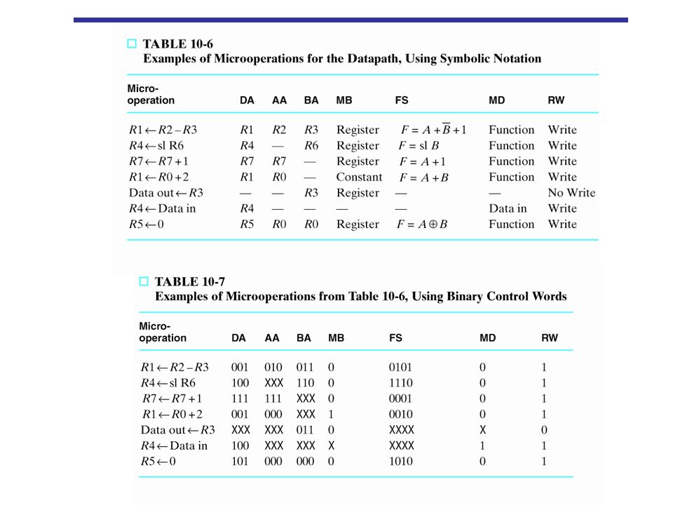
Control word Example: RR2+R3’+1 Field: DA AA BA MB FS MD RW
R2 is the A input of ALU R3 is the B input of ALU Operation to be performed is A+B’+1 R1 is the destination register RW should be 1 to cause R1 to be written Field: DA AA BA MB FS MD RW Binary:

19
Simple computer architecture
Programmable systems: can execute programs In a programmable system a portion of the input consists of sequence of instructions. Instruction specifies the operation to be preformed, which operands to use, where to place the results. To execute the instructions in sequence, the address of the instruction to be performed is required This address comes from a register called program counter (PC). Executing an instruction means activating the necessary sequence of microoperations in the datapath required to perform the instruction
. Executing an instruction means activating the necessary sequence of microoperations in the datapath required to perform the instruction.")
20
Simple computer architecture
User specifies operations to be performed and their sequence using a program Program: list of instructions that specifies operations, operands and the sequence Control unit reads an instruction from the memory and decodes and executes the instruction by issuing a sequence of microoperations. Ability to execute a program from memory is the most important property of a general purpose computer

21
Simple computer architecture
Instruction: a collection of bits that instruct the computer to perform a specific operation Collection of instructions for a computer is called instruction set An instruction is usually depicted by a rectangular box symbolizing the bits of the instruction The bits are divided into groups called fields Operation code of an instruction (opcode) is a group of bits in the instruction that specifies an operation (add, subtract, shift)
 is a group of bits in the instruction that specifies an operation (add, subtract, shift)")
22
Simple computer architecture
The operation must be performed using data stored in computer registers or in memory An instruction must specify not only the operation but also the registers or memory in which the operands are to be found and the result to be placed We will consider a simple computer as an example.

23
Simple computer architecture

24
Simple computer architecture
Our simple computer has 8 registers (R0-R7), three bits require to identify each Three instruction formats for the simple computer are illustrated here. First instruction format: an opcode, a destination register (DR) a source register A (SA) and a source register B (SB) Second instruction format: an opcode, a destination register, a source register and an operand Third instruction format: does not change any register, instead affects the order in which the instructions are fetched from memory
, three bits require to identify each. Three instruction formats for the simple computer are illustrated here. First instruction format: an opcode, a destination register (DR) a source register A (SA) and a source register B (SB) Second instruction format: an opcode, a destination register, a source register and an operand. Third instruction format: does not change any register, instead affects the order in which the instructions are fetched from memory.")
25
Simple computer architecture

26
Simple computer architecture

27
Simple computer architecture
Location of an instruction to be fetched is determined by the program counter (PC). Ordinary PC fetches instruction from sequential addresses but a jump can be achieved if the content of PC is changed Third instruction format can create jump, it has an opcode, one register field, and a split address field (AD) If based on the content of the register jump has to occur, the address of new location from which the next instruction is to be fetched, is formed by adding current PC and the content of 6 bit address field
. Ordinary PC fetches instruction from sequential addresses but a jump can be achieved if the content of PC is changed. Third instruction format can create jump, it has an opcode, one register field, and a split address field (AD) If based on the content of the register jump has to occur, the address of new location from which the next instruction is to be fetched, is formed by adding current PC and the content of 6 bit address field.")
28
Simple computer architecture
6 bit address is treated as a signed two’s complement To preserve two’s complement representation, signed extension is applied to 6 bit address to form a 16 bit offset Signed extension: if the leftmost bit of the address field is a 1, then 10 bits to its left are filled with 1’s to give a negative two’s complement offset. if the leftmost bit of the address field is a 0, then 10 bits to its left are filled with 0’s to give a positive two’s complement offset. Example: PC=55, a branch is to occur to location 35 if the content of R6 is zero. Opcode will be a branch on zero, SA would be specified as R6 and AD would be 6-bit two’s complement of -20.

29
Instruction Specifications
Instruction specification: describe each of the instructions that can be executed by the system Mnemonic format: symbolic representation for the opcode Mnemonic format is converted to binary representation by a program called assembler

30
Single-cycle computer
Single cycle computer: a computer that fetches and executes an instruction in a single clock cycle PC provides instruction address to instruction memory, instruction output from the instruction memory goes to control logic (instruction decoder) Output of instruction memory also goes to Extend and Zero fill. Extend: provides address offset to the PC Append leftmost bit of 6-bit address offset field AD to the left of AD, preserving two’s complement representation Zero fill: provides constant input to datapath Appends 13 zeros to the left of the OP field of the instruction
 Output of instruction memory also goes to Extend and Zero fill. Extend: provides address offset to the PC. Append leftmost bit of 6-bit address offset field AD to the left of AD, preserving two’s complement representation. Zero fill: provides constant input to datapath. Appends 13 zeros to the left of the OP field of the instruction.")
31
Single-cycle computer
PC is updated in each clock cycle Behavior of PC is determined by opcode, N and Z. If a jump occures, new PC value is the value on bus A. If a branch is taken, new PC value is sum of previous PC value and sign-extended address offset Otherwise PC is incremented by 1 A jump occurs for bit 13 in the instruction equal to 1 A branch occurs for bit 13 in the instruction equal to 0 Condition for branch is selected by bit 9 of instruction bit 9 equal to 1: N is selected bit 9 equal to 0: Z is selected

32
Single-cycle computer

33
Single-cycle computer

34
Single-cycle computer
Instruction decoder is a combinational circuit that provides all of the control words for datapath based on the content of the fields of the instruction. Some of the fields of control word can be obtained directly from the content of the fields in the instruction DA, AA and BA are equal to the instruction fields DR, SA and SB. BC (for selection of branch condition status bits) is taken directly from last bit of Opcode.
 is taken directly from last bit of Opcode.")
35
Single-cycle computer

36
Single-cycle computer
In order to design the decoder logic, we divide the various instructions possible for the simple computer into different types and then assign the first three bits of the opcode to various types. The types assignment are based on the use of specific hardware such as MUX B, Function unit, Register file, ….

37
Single-cycle computer
Six instruction for our simple computer are listed in Table 10.11 Suppose output of the instruction memory is the first instruction, “Add Immediate” Based on the first three bits of opcode, 100, outputs of instruction decoder will be: MB=1, MD=0, RW=1, MW=0 Last three bits of instruction are extended to 16 bits by zero fill Since MB=1, this zero-filled value is placed on bus B MD=0, the function unit output is selected Since the last four bits of the opcode are 0010, the operation is A+B

38
Single-cycle computer
Zero-filled value on bus B is added to content of register SA, with the results presented on bus D Since RW=1, value on bus D is written to register DR Since MW=0, no write to memory occurs The entire operation takes place in a single clock cycle Since PL=0, PC is incremented

39
Single-cycle computer
Second instruction: LD (load from memory), opcode First three bits 001 gives: MD=1, RW=1 MW=0 These values and SA and DR fully specify the instruction: load the content of memory address specified by SA into register DR. PL=0 so PC is incremented JB and BC are ignored since this is neither a jump not a branch
, opcode First three bits 001 gives: MD=1, RW=1 MW=0. These values and SA and DR fully specify the instruction: load the content of memory address specified by SA into register DR. PL=0 so PC is incremented. JB and BC are ignored since this is neither a jump not a branch.")
40
Single-cycle computer
Third instruction, ST First three bits of opcode 010 give control signals: MB=0, RW=0, MW=1 MW=1 causes a memory write operation with address and data from the register file RW=0 prevents writing to register file Address for the memory write comes from the register selected by field SA and data for memory write comes from register selected by SB, since MB=0 DR is not used since no write occurs to a register

41
Single-cycle computer
Sixth instruction is a conditional branch and manipulates the PC value PL=1, so the PC is loaded instead of incremented JB=0 causing a conditional branch rather than a jump Since BC=0, register R[SA] is tested for a value of zero If R[SA]=0 the PC value becomes PC +se AD (se means sign extended), otherwise PC is incremented DR and SB fields become 6-bit address fields AD which is sign extended and added to PC
, otherwise PC is incremented. DR and SB fields become 6-bit address fields AD which is sign extended and added to PC.")
42
Single-cycle computer
Example: write a program for our simple computer to calculated 83-(2+3). Assume that register R3 contains 248, location 248 in data memory contains 2, location 249 contains 83, and the result is to be place in location 250. LD R1, R3 ADI R1, R1, 3 NOT R1, R1 INC R1, R1 INC R3, R3 LD R2, R3 ADD R2, R2, R1 ST R3, R2
. Assume that register R3 contains 248, location 248 in data memory contains 2, location 249 contains 83, and the result is to be place in location 250. LD R1, R3. ADI R1, R1, 3. NOT R1, R1. INC R1, R1. INC R3, R3. LD R2, R3. ADD R2, R2, R1. ST R3, R2.")
43
Single-cycle computer

44
Multiple-cycle computer
Single-cycle computer is not able to perform complex operations (operations that cannot be completed in one clock cycle such as multiplication) Single cycle computer has two separate 16-bit memories for instructions and data. For a simple computer with instructions and data in the same 16-bit memory, two read accesses of memory are required (one to load the instruction and one to read or write the data) Since two different addresses must be applied to the memory address inputs, at least two clock cycles are required.
 Single cycle computer has two separate 16-bit memories for instructions and data. For a simple computer with instructions and data in the same 16-bit memory, two read accesses of memory are required (one to load the instruction and one to read or write the data) Since two different addresses must be applied to the memory address inputs, at least two clock cycles are required.")
45
Multiple-cycle computer
Single cycle computer has a longer worst case delay path and therefore a lower limit on the clock frequency

46
Multiple-cycle computer

47
Multiple-cycle computer
We modify the architecture of the simple computer to a multiple-cycle computer Separate instruction memory and data memory are replaced with memory M. To fetch instructions, PC is the address source for memory and to fetch data, Bus A is the address source. MUX M selects between these two address sources MUX M requires an additional control signal MM which is added to the control word format Since instructions from M are needed in the control unit, a path is added from its output to the instruction register IR.

48
Multiple-cycle computer
In executing an instruction across multiple clock cycles, data generated during current cycle if often needed in a later cycle. This data can be temporarily stored in a register. Registers used for temporary storage are usually not visible to the user Second modification provides these temporary registers by doubling the number of registers in register file. Registers 8 to 15 are temporary registers

49
Multiple-cycle computer
During execution of a multiple-cycle instruction, PC must be held at its current value for all but one of the cycles. To provide this hold capability, the PC is modified to be controlled by a 2-bit control word, PS. Because of multiple cycles, instruction need to be held in a register for use during its execution since its value may be needed for more than just the first cycle. Register used for this purpose is the instruction register IR Since IR load only when an instruction is being read from memory, it has a load-enable signal IL that is added to the control word.

50
Multiple-cycle computer
Because of multiple-cycle operation, a sequential control circuit, which can provide a sequence of control words for microoperations used to interpret the instruction is required and replaces the Instruction decoder. The sequential control unit consists of the Control state register and the combinational Control logic Control logic has state, opcode and status bits as its inputs and produces control word as its output. Conceptually, control word is divided into two parts, one for sequence control, which determines the next state of the overall control unit, and one for Datapath control, which controls the microoperations executed by Datapath and Memory.

51
Multiple-cycle computer
DX, AX, BX control register selection. If the MSB of one of these fields is ), corresponding register address DA, AA or BA is that given by DR, SA and SB. If the MSB of one of these fields is 1, corresponding register address is the content of fields DX, AX or BX. This selection process is performed by Register address logic, which contains three multiplexers (one for each of DA, AA, BA) controlled by the MSB of DX, AX and BX.
, corresponding register address DA, AA or BA is that given by DR, SA and SB. If the MSB of one of these fields is 1, corresponding register address is the content of fields DX, AX or BX. This selection process is performed by Register address logic, which contains three multiplexers (one for each of DA, AA, BA) controlled by the MSB of DX, AX and BX.")
52
Multiple-cycle computer

53
Multiple-cycle computer
NS in the control word provides the next state for the Control State register The 2-bit PS field controls the program counter PC (00 holds its state, 01 increment by 1, 10 load PC plus sign-extended AD, 11 load the contents of R[SA]. Instruction register is loaded only once during execution of an instruction (IL=1 new instruction loaded, IL=0 instruction remains unchanged)
")
54
Multiple-cycle computer
Sequential control unit consists of Control state register and combinational Control logic. Design of the sequential control logic can be performed by developing its ASM chart and finding the state table using the chart. We first develop ASM chart for instructions that can be implemented with minimum number of clock cycles. For instructions requiring memory access for data as well as instruction, at least two clock cycles are required: instruction fetch and instruction execution

55
Multiple-cycle computer

56
Multiple-cycle computer
Instruction fetch occurs in state INF PC has the address of instruction in memory M. This address is applied to the memory, and the word read from memory is loaded into IR. In state EX0 the instruction is decoded by a vector decision and the microoperations executing the instruction appear in conditional boxes. For instructions that do not change PC content, PC is incremented. Example: opcode for ADD instruction adds the content of register specified by SA to content of register specified by SB and writes the result into register specified by DR

57
Multiple-cycle computer
Example: opcode is load instruction (LD), which uses value in register specified by SA for the address and loads the data word from memory M into register specified by DR Example: opcode is branch on negative (BRN) instruction. Decoding of this instruction causes the value in register specified by SA to be passed through the Function unit in order to evaluate status bits N and Z. N and Z then propagate back to Control logic Based on value of N, the branch is taken or not taken by adding the extended address AD from the instruction to the value of PC or incrementing PC
, which uses value in register specified by SA for the address and loads the data word from memory M into register specified by DR. Example: opcode is branch on negative (BRN) instruction. Decoding of this instruction causes the value in register specified by SA to be passed through the Function unit in order to evaluate status bits N and Z. N and Z then propagate back to Control logic. Based on value of N, the branch is taken or not taken by adding the extended address AD from the instruction to the value of PC or incrementing PC.")
58
Multiple-cycle computer
An example of an instruction that cannot be completed in two cycles is “load register indirect” (LRI). In this instruction, content of register R[SA] addresses a word in memory. The word, known as indirect address, is then used to address the word in memory that is loaded into register R[DR] R[Dr]M[M[R[SA]]]
. In this instruction, content of register R[SA] addresses a word in memory. The word, known as indirect address, is then used to address the word in memory that is loaded into register R[DR] R[Dr]M[M[R[SA]]]")
59
Multiple-cycle computer
Following instruction fetch, state becomes EX0. In this state R[SA] addresses the memory to obtain the indirect address which is then placed in register R8. In the next state, EX1, next memory access occurs with address from R8. The operand is placed in R[DR] to complete the operation and PC is incremented.

Similar presentations


 contains datapath unit and control unit. Datapath: A.>")


 Montek Singh April 9, 2007.>")


 Terms of Use Chapter 10 – Computer.>")


