Download presentation
Presentation is loading. Please wait.

1
Chapter 12 : Field – Effect Transistors 12-1 NMOS and PMOS transistors 12-2 Load-line analysis of a simple NMOS amplifier 12-3 Small –signal equivalent circuits 12-4 Common source amplifiers 12-5 Source followers 12-6 CMOS logic gates

2
MOSFET Transsistors

3
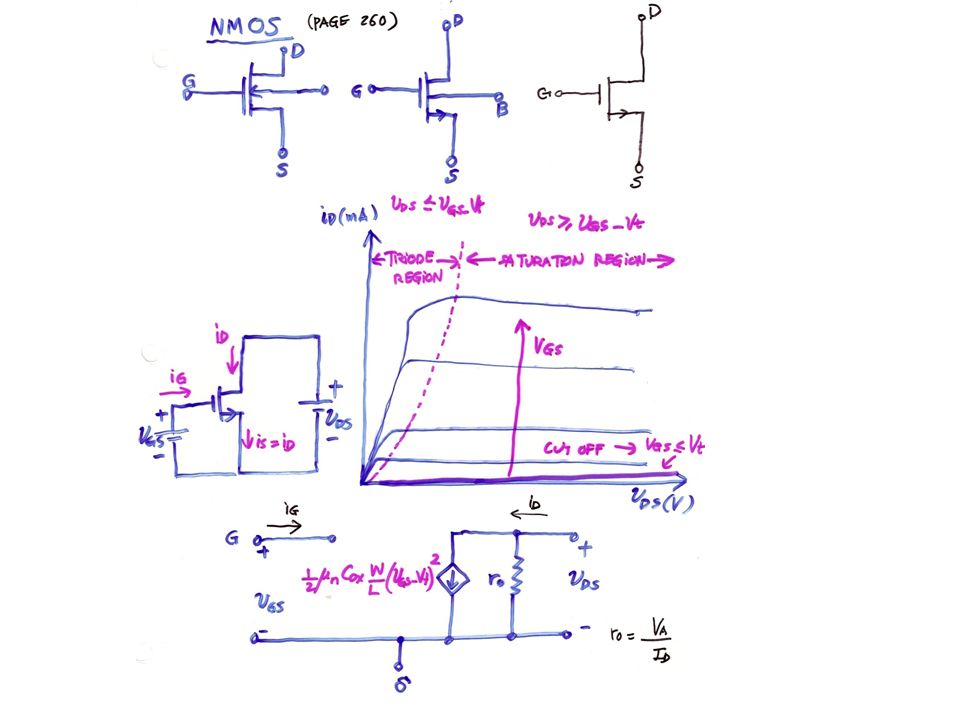
N-channel enhancement MOSFET

4
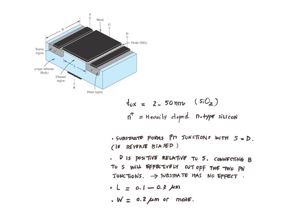
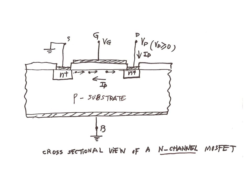
4-1. Device Structure. Fig. 4-1. Physical structure of the enhancement- type NMOS transistor

6
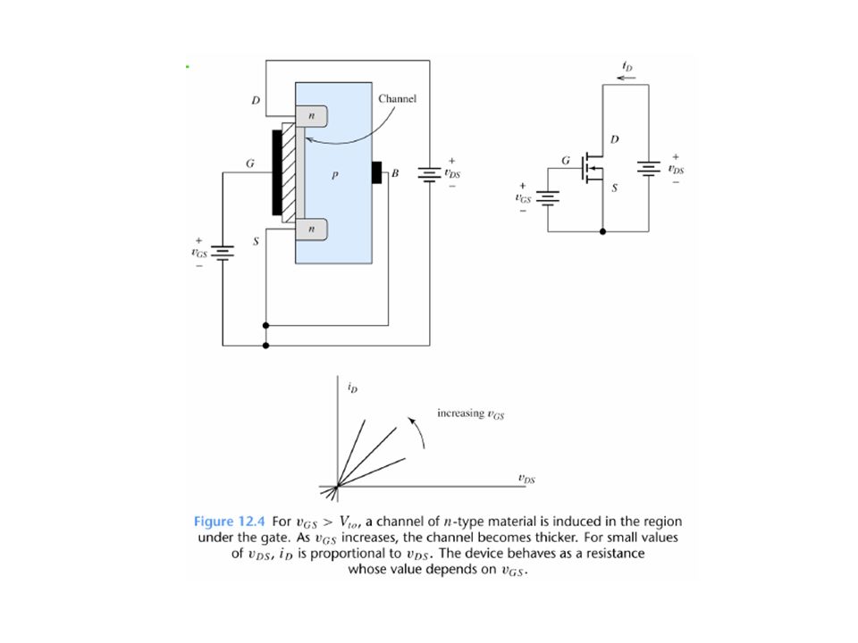
Fig. 4-2. The enhancement-type NMOS transistor with applied voltage

8
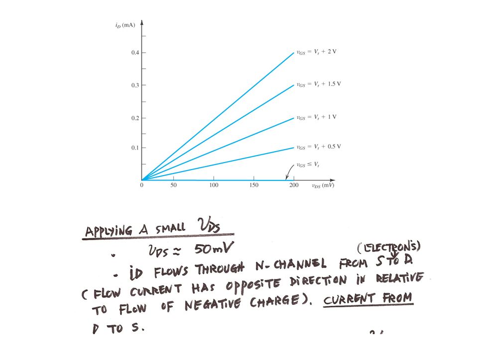
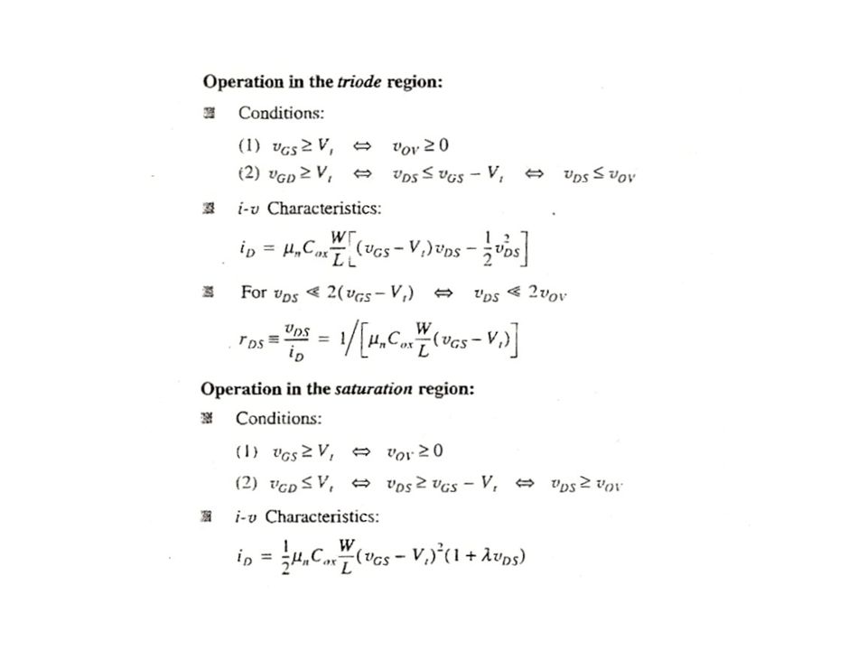
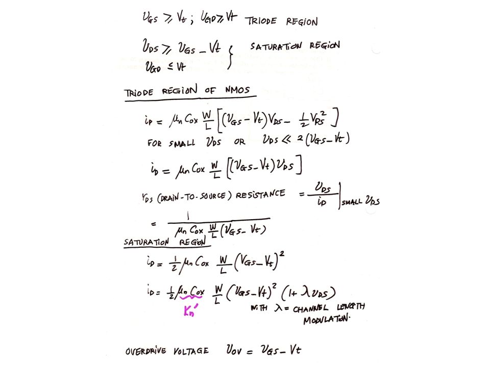
Applying a small v DS. Fig. 4-3 An NMOS transistor with v GS > v t and s small v DS

13
Operation in the cut - off

17
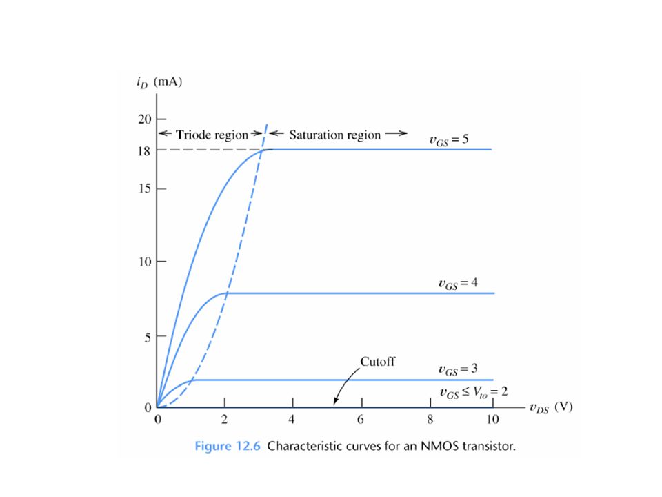
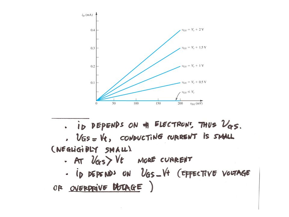
Fig. 4-4. The i D –v DS characteristics of the MOSFET

21
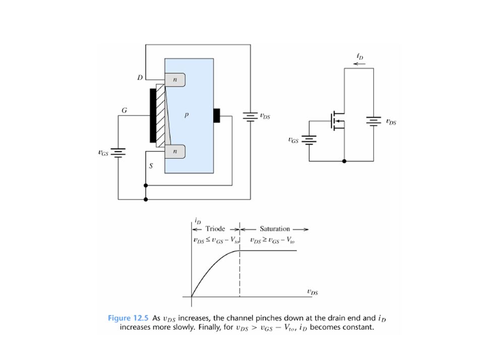
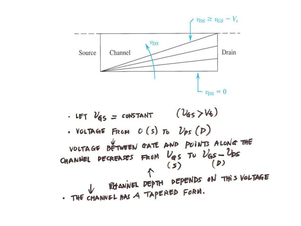
With increasing v DS. Fig. 4-5 The enhancement NMOS transistor as v DS is increased

22
Fig. 4-6 The drain current i D vs v DS

23
Fig. 4-11 The i D – v DS characteristics of an n- channel enhancement type MOSFET

24
Fig. 4-12 The i D -v DS characteristic for an enhancement –type NMOS transistor in saturation

25
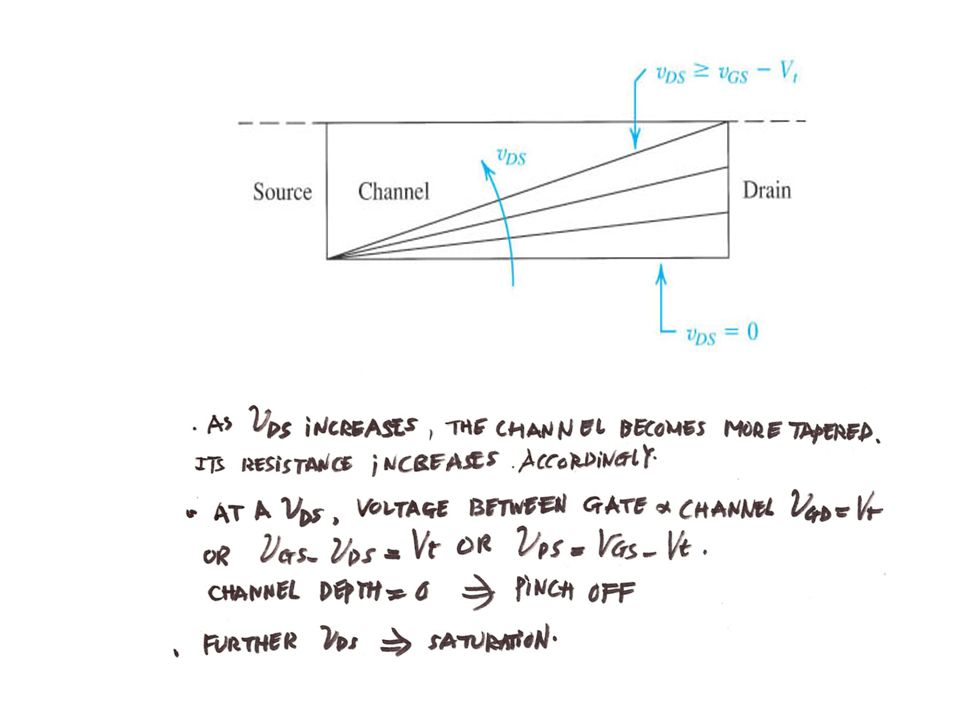
Fig. 4-7 A tapered shape caused by increasing v DS

30
Fig. 4-10 Circuit symbol for the n-channel enhancement –type MOSFET

31
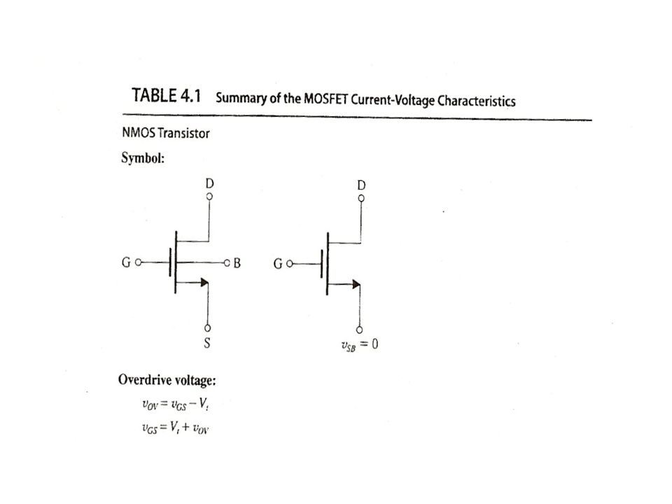
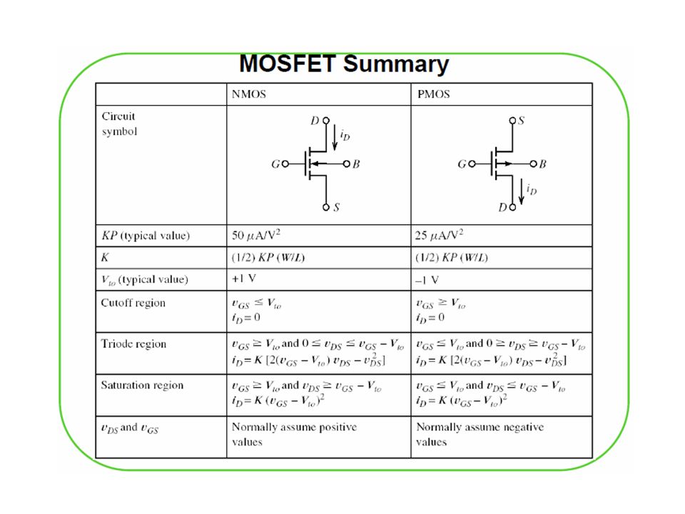
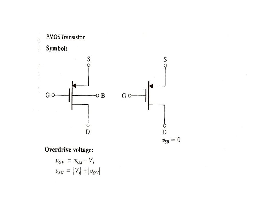
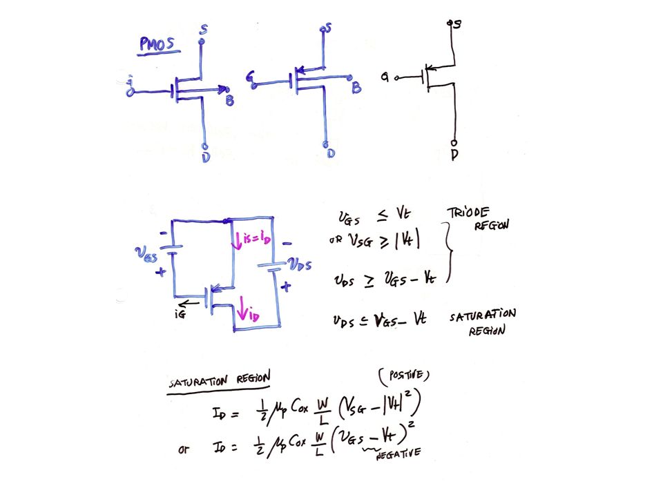
The p-Channel MOSFET v GS, v DS and v t are negative i D enters from the source terminal and leaves through the drain terminal. NMOS operates faster and at lower power than PMOS.

47
Fig. 4-13 Large signal equivalent circuit of an n- channel MOSFET

48
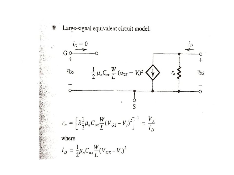
Fig. 4-17 Large signal equivalent circuit of the n- channel MOSFET in saturation with r 0

49
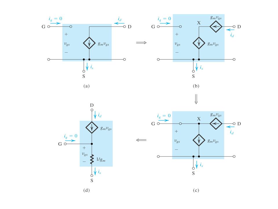
Fig. 4-37 Small signal models for the MOSFET

50
Fig. 4-37 (b) with the channel length modulation
 with the channel length modulation")
52
Fig. 4-40 T model of the MOSFET with r 0

53
Chapter 12 : Field – Effect Transistors 12-1 NMOS and PMOS transistors 12-2 Load-line analysis of a simple NMOS amplifier 12-3 Small –signal equivalent circuits 12-4 Common source amplifiers 12-5 Source followers 12-6 CMOS logic gates

55
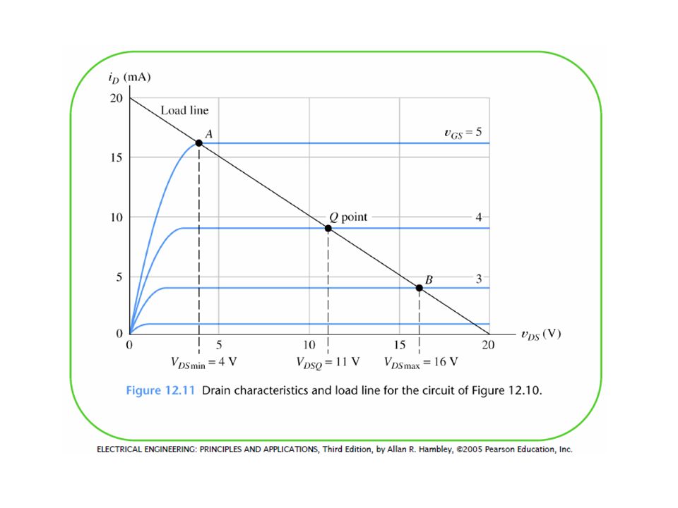
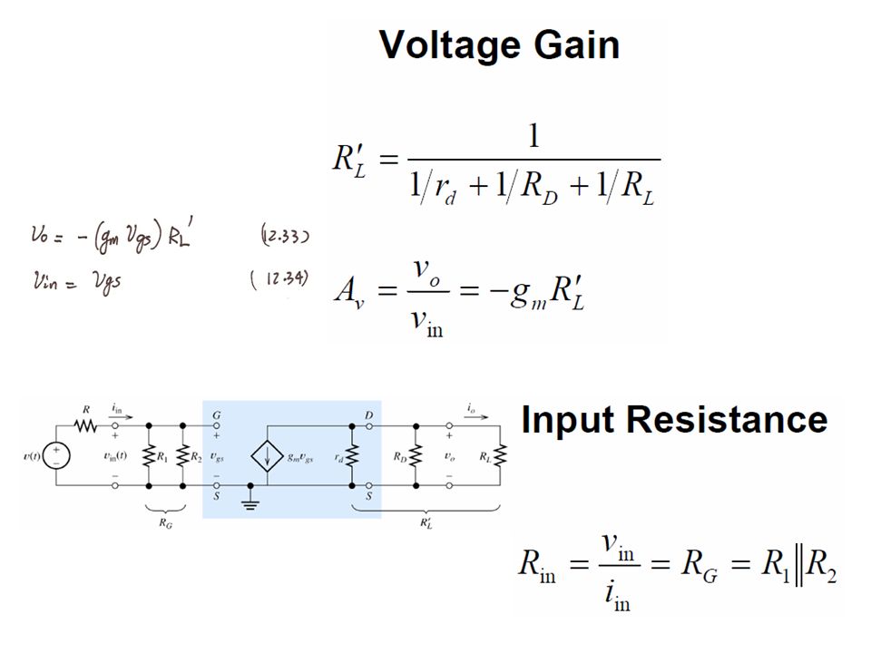
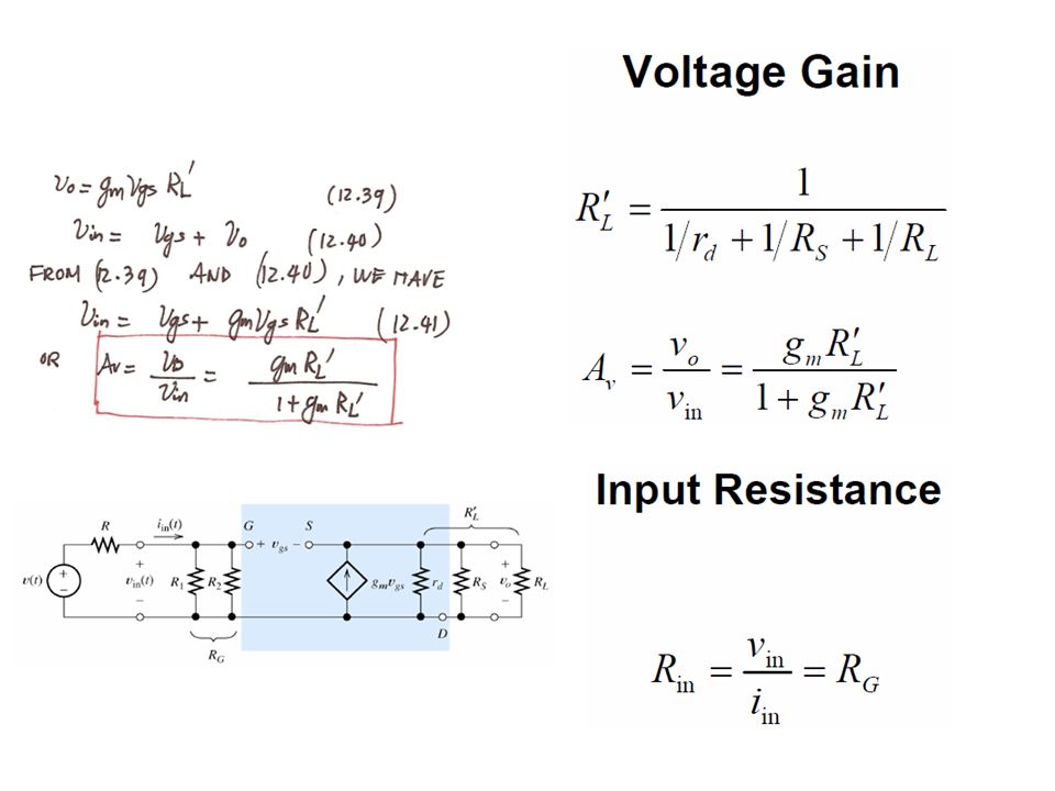
Common- source amplifiers

77
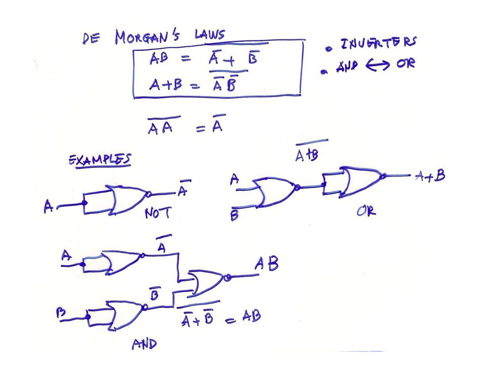
10.3 CMOS Logic Gate Circuits 10.3.1 Basic structure Fig. 10.8 Representation of a three- input CMOS logic gate

Similar presentations


 Field-Effect Transistors (FET) MOSFET Introduction 1.>")


>")


>")
>")
 perspective view; (b) cross section. Typically L = 1 to 10 m, W = 2 to 500.>")
 Importance for LSI/VLSI –Low fabrication cost –Small size –Low power consumption Applications –Microprocessors –Memories.>")
>")


>")