Download presentation
Presentation is loading. Please wait.

1
© 2008, Renesas Technology America, Inc., All Rights Reserved 1 Course Introduction Purpose This training course provides an overview of the CPU architecture of the MCUs in the M16C/2x and M16C/6x series. Objectives Learn the interrupt sources on M16C series devices. Understand a detailed interrupt sequence, including the source and magnitude of interrupt latencies and interrupt priorities. Understand the advantage of two stack pointers. Learn how to minimize Interrupt Service Routine execution time and nest interrupts. Content 16 pages 3 questions Learning Time 25 minutes

2
© 2008, Renesas Technology America, Inc., All Rights Reserved M16C/60 CPU Core/Register Model R0HR0L R1HR1L R2 R3 A0 A1 FB 08 / 0 0 0 0 0 16 / 0 015 31 / 15 15 15 / 7 7 7 8 bits 16 bits SB 015 ISP USP 0 015 FLG PC INTB 0 0 0 19 15 20 bits Data Registers 2 x 32-bit registers ( R0R2, R1R3 ) or 4 x 16-bit registers ( R0, R1, R2, R3 ) or 4 x 8-bit registers ( R0L, R0H, R1L, R1H ) Address Registers 2 x 16-bit Address / General-Purpose Register A0, A1 1 x 32-bit Address Register [ A0A1 ] Base Registers SB and FB registers can be used in indexed addressing modes (e.g., C-language stack frame addressing) Control Registers 2 stack pointers allow H/W interrupt stack and OS stack Flag Register – Condition flags and interrupt priority 20-bit Program Counter Interrupt Table Pointer allows multiple Interrupt Vector Tables
![© 2008, Renesas Technology America, Inc., All Rights Reserved M16C/60 CPU Core/Register Model R0HR0L R1HR1L R2 R3 A0 A1 FB 08 / / / / bits 16 bits SB 015 ISP USP FLG PC INTB bits Data Registers 2 x 32-bit registers ( R0R2, R1R3 ) or 4 x 16-bit registers ( R0, R1, R2, R3 ) or 4 x 8-bit registers ( R0L, R0H, R1L, R1H ) Address Registers 2 x 16-bit Address / General-Purpose Register A0, A1 1 x 32-bit Address Register [ A0A1 ] Base Registers SB and FB registers can be used in indexed addressing modes (e.g., C-language stack frame addressing) Control Registers 2 stack pointers allow H/W interrupt stack and OS stack Flag Register – Condition flags and interrupt priority 20-bit Program Counter Interrupt Table Pointer allows multiple Interrupt Vector Tables](http://images.slideplayer.com/33/8171396/slides/slide_2.jpg "© 2008, Renesas Technology America, Inc., All Rights Reserved M16C/60 CPU Core/Register Model R0HR0L R1HR1L R2 R3 A0 A1 FB 08 / / / / bits 16 bits SB 015 ISP USP FLG PC INTB bits Data Registers 2 x 32-bit registers ( R0R2, R1R3 ) or 4 x 16-bit registers ( R0, R1, R2, R3 ) or 4 x 8-bit registers ( R0L, R0H, R1L, R1H ) Address Registers 2 x 16-bit Address / General-Purpose Register A0, A1 1 x 32-bit Address Register [ A0A1 ] Base Registers SB and FB registers can be used in indexed addressing modes (e.g., C-language stack frame addressing) Control Registers 2 stack pointers allow H/W interrupt stack and OS stack Flag Register – Condition flags and interrupt priority 20-bit Program Counter Interrupt Table Pointer allows multiple Interrupt Vector Tables")
3
© 2008, Renesas Technology America, Inc., All Rights Reserved 3 Interrupt Sources of M16C Family Hardware Interrupt Software Interrupt Bus collision detection Block transmit A-D conversion Serial I/O Timer Key input External pin DMA1 DMA0 UART2/NACK transmit UART2/ACK receive UART1 trans & rec UART0 trans & rec Timer A4 to A0 Timer B5 to B0 INT5 to 0 Peripheral I/O Reset NMI DBC Watchdog timer Single step Address match Address match interrupt 1 Address match interrupt 0 BRK instruction INT instruction INT0 instruction (overflow/0 divide) UND instruction (Undefined instruction) SI/O4 trans & rec SI/O3 trans & rec Special
 UND instruction (Undefined instruction) SI/O4 trans & rec SI/O3 trans & rec Special")
4
© 2008, Renesas Technology America, Inc., All Rights Reserved 4 Interrupt Vector Tables Locations of interrupt service routines are stored in Vector Tables Two types of Interrupt Vector Tables are used: - Fixed Vector Table – starting location of the vector table is fixed - Variable Vector Table – starting location of the vector table is set by the value in the Interrupt Table Register (INTB) Low Address Mid Address XXXX High Address XXXX Format of Interrupt Vector Address in Vector Table MSB LSB Table Address + 1 Table Address + 0 Table Address + 2 Table Address + 3
 Low Address Mid Address XXXX High Address XXXX Format of Interrupt Vector Address in Vector Table MSB LSB Table Address + 1 Table Address + 0 Table Address + 2 Table Address + 3")
5
© 2008, Renesas Technology America, Inc., All Rights Reserved 5 Fixed Vector Table Interrupt SourceVector Table Addresses Remarks Undefined InstructionFFFDC16 to FFFDF16Interrupt on UND Instruction OverflowFFFE016 to FFFE316Interrupt on INTO Instruction BRK InstructionFFFE416 to FFFE716If the vector is FFFFFF, vector is found in variable vector table Address MatchFFFE816 to FFFEB16There is an address-matching interrupt enable bit Single Step*FFFEC16 to FFFEF16Do Not Use Watchdog TimerFFFF016 to FFFF316Also Oscillation Stop Detect on devices with that feature DBC*FFFF416 to FFFF716Do Not Use NMIFFFF816 to FFFFB16External Interrupt to NMI pin RESETFFFFC16 to FFFFF16 * Interrupts used for debugger purposes only

6
© 2008, Renesas Technology America, Inc., All Rights Reserved 6 Variable Vector Table 0 1 2 62 63 Software Interrupt Number Variable Vector Table (256 bytes) Address INTB One vector consists of 4 bytes, so 63 vector locations are specified. Interrupt table register sets start address.

7
© 2008, Renesas Technology America, Inc., All Rights Reserved 7 Variable Vector Table Example: If INTB = FFC00 16, then Timer B5 Interrupt vector starts at FFC14 16 Peripheral Interrupt Vectors

9
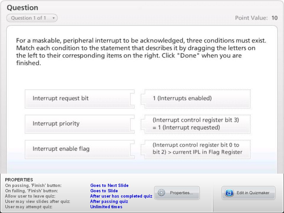
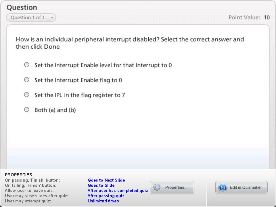
© 2008, Renesas Technology America, Inc., All Rights Reserved 9 Interrupt Generation Conditions Interrupt request bit (Interrupt control register bit 3) = 1 (Interrupt requested) Interrupt priority (Interrupt control register bit 0 to bit 2) > current IPL in Flag Register (3) Interrupt enable flag = 1 (Interrupts enabled) IPL b15 Interrupt Control Register (typical) Each maskable interrupt has an interrupt control register for setting the interrupt’s priority and a local request bit. (The request bit is set by the interrupt condition.) When all of the following conditions occur, an interrupt is generated: 4-7 3 2 1 0 BitFunction Bit Name Symb ol Nothing is assigned This bit can be read, but only be written to 0 Interrupt Request bit IR ILVL2 ILVL1 The value given by these three bits set interrupt priority. Set to 0 to disable interrupt Interrupt Priority Level Select bit ILVL0 Reserved b14-b12 b11-b8 U b7 I OB Z D C b0 FLAG Register S (2) (1)
 When all of the following conditions occur, an interrupt is generated: BitFunction Bit Name Symb ol Nothing is assigned This bit can be read, but only be written to 0 Interrupt Request bit IR ILVL2 ILVL1 The value given by these three bits set interrupt priority. Set to 0 to disable interrupt Interrupt Priority Level Select bit ILVL0 Reserved b14-b12 b11-b8 U b7 I OB Z D C b0 FLAG Register S (2) (1).")
11
© 2008, Renesas Technology America, Inc., All Rights Reserved 11 Interrupt Latency 1. Time “a” is variable. This is the time to finish the current instruction. Typically, it’s 3 cycles or less. The worst-case delay is 30 cycles for the DIVX instruction. 2. Time “b” is 18 cycles with an even address vector and SP with a 16-bit bus. It is 19 cycles if either the SP or vector address is odd, or 20 cycles if both are odd. 3. Return from Interrupt (REIT) is 6 cycles.
 is 6 cycles..")
12
© 2008, Renesas Technology America, Inc., All Rights Reserved 12 Interrupt Sequence 1. The CPU gets the interrupt information (interrupt cause and interrupt level) from address 0. 2. The Flag register is saved to an internal area. 3. The Interrupt Enable (I), Debug (D), and Stack Pointer Select (U) flags are cleared. (The U flag doesn’t change for interrupt numbers 32 - 63 of the INT instruction.) 4. The flag contents from the temporary register are saved to the stack, along with the program counter. 5.The interrupt request bit for the acknowledged interrupt is cleared. 6.The IPL in the flag register is set to that of the acknowledged interrupt. - For the WDT and NMI interrupts, the priority is set to 7 - A RESET forces the IPL to 0 7.The Program Counter is loaded with the location of the Interrupt Service Routine.
 from address The Flag register is saved to an internal area. 3. The Interrupt Enable (I), Debug (D), and Stack Pointer Select (U) flags are cleared. (The U flag doesn’t change for interrupt numbers of the INT instruction.) 4. The flag contents from the temporary register are saved to the stack, along with the program counter. 5.The interrupt request bit for the acknowledged interrupt is cleared. 6.The IPL in the flag register is set to that of the acknowledged interrupt. - For the WDT and NMI interrupts, the priority is set to 7 - A RESET forces the IPL to 0 7.The Program Counter is loaded with the location of the Interrupt Service Routine..")
13
© 2008, Renesas Technology America, Inc., All Rights Reserved 13 Task B Task C Task A Task B (USP) Task C (USP) Task A (USP) Stack for interrupt (ISP) For interrupt Higher RAM use efficiency, less time optimizing One-stack-pointer system Two-stack-pointer system For interrupt Task Stack Space Two stack pointers eliminate need to have redundant interrupt space reserved in each task’s stack area. Interrupt Stack Space Two SPs for Multitasking Systems

14
© 2008, Renesas Technology America, Inc., All Rights Reserved 14 Interrupt Service Routines Bank Switching — Using the Alternate Register Set - To create very fast Interrupt Service Routines (ISRs), use the M16C register-bank switching feature instead of PUSHM and POPM. - The bank switching can be automatically controlled by the compiler by utilizing the /B option when declaring the interrupt. - Bank switching should typically NOT be used in an ISR that can be nested. Nesting Interrupts - The MCU hardware clears the Interrupt Enable Flag (I bit) when an interrupt is accepted. To allow interrupts to occur within an ISR, the service routine must re-enable interrupts (set the I bit). - If the interrupt is declared using the /E option, the compiler will re- enable interrupts during the interrupt service routine.
 when an interrupt is accepted. To allow interrupts to occur within an ISR, the service routine must re-enable interrupts (set the I bit). - If the interrupt is declared using the /E option, the compiler will re- enable interrupts during the interrupt service routine..")
16
© 2008, Renesas Technology America, Inc., All Rights Reserved 16 Course Summary Interrupt sources on M16C series devices Fixed and Variable Interrupt Vector tables Interrupt sequence, including the source and magnitude of interrupt latencies and interrupt priorities Advantage of having two stack pointers Nesting Interrupts and using the Bank Switching feature

Similar presentations


 is needed. Sources of interrupts: internal fault (e.g.. divide by.>")


