Download presentation
Presentation is loading. Please wait.

1
Chapter 10 Fundamentals of Wafer-Level Packaging Jason Mucilli Vincent Wu October 1, 2007

2
What is Wafer-Level Packaging? IC packaging formed at the wafer level on the wafer in the wafer foundry Front end IC fabrication and back end IC assembly performed at wafer foundry CSP (chip-scale package) 20% larger than IC’s-done ass single chip packages at IC level, assembled by standard SMT, encapsulated and tested Flip Chip Done at wafer level and solder bonded with face down Wafer level packaging Goes extra step in forming electrical connections on the wafer, assembled face down but with SMT equipment, then encapsulating, testing and singulating as packaged IC’s
 20% larger than IC’s-done ass single chip packages at IC level, assembled by standard SMT, encapsulated and tested Flip Chip Done at wafer level and solder bonded with face down Wafer level packaging Goes extra step in forming electrical connections on the wafer, assembled face down but with SMT equipment, then encapsulating, testing and singulating as packaged IC’s.")
3
What is Wafer-Level Packaging? Cont. Today’s wafer and IC packaging vs. new wafer level packaging process:

4
Why Wafer-level packaging? Possible benefits Smallest system size Enabling interconnect continuum from IC to PWB because of thin-film processing Reduced cost of packaging, testing and burn-in because all done at the wafer level Elimination of underfill because compliancy of leads or other ways to achieve reliability Improved electrical performance due to short lead lengths

5
Why Wafer-level packaging? Cont. Size benefits Shrinking size of portable and hand-held electronic devices Ultimate IC packaging option-the package and the area it occupies on the PWB are equal to the size of an IC

6
Why Wafer-level packaging? Cont. Cost benefits-achieved by 2 techniques: Increasing wafer size results in more IC’s per wafer Decreasing feature size on the IC- causes “die- shrinks” which result in more IC’s for a given wafer size Equipment Costs As wafer gets larger, the cost of the equipment also goes up Cost increase is more than offset by increased production capacity

7
Disadvantages Incompatibility of PWB Very high I/O IC’s would require very small solder balls on a very tight pitch Requires very high density PWB to interconnect- expensive

8
Why Wafer-level packaging? Cont. Disadvantages Cont. ALL the IC’s (good and bad) are packaged at the wafer level Results in bad IC’s packaged early on when yields are low
 are packaged at the wafer level Results in bad IC’s packaged early on when yields are low.")
9
WLP Technologies Evolution of the Silicon wafer in size 30 years ago-82.5mm Now-300mm Factor of 10 in IC productivity-also drives down cost

11
WLP Technologies Cont. More than a dozen different ways of forming wafer-level packages: 3 categories Redistributing WLP Encapsulated WLP Flex/Tape WLP

12
Redistribution of WLP Technologies WLP Processes Redistribution Flip-Flop technology Figure 10.10

13
Redistribution of WLP Technologies cont.

16
Redistribution technology offers protection WLP technology use same technology as flip chip or bare die direct chip attachment to organic board Difference in solder balls size

17
Encapsulated WLP Technologies Encapsulated technology Seals the chip between glass plates. Peripheral Pads Technology and material similar to redistribution. Wafer Front and Backside Thickness lithography

18
Encapsulated WLP Technologies

19
Flex Tape WLP Technologies Flex Tape WLP Conventional flex tape Copper-polyimide flex tape Wafer IC Connected by wirebonding Liquid encapsulant protection

20
Flex Tape WLP Technologies cont.

21
WLP Reliability Fundamentals of reliability Coffin-Mason Modified Equation Reliable connection Four Ways

22
WLP Reliability cont. Has been used for over 30 years.

23
Need for Underfill in WLP WLP IC packaging technology at wafer level w/o underfill is reliable. But… Interconnection b/w IC board rigid connection Ex. Solder

24
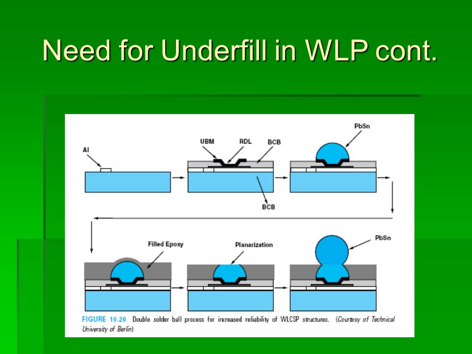
Need for Underfill in WLP cont. Underfill Distributes stress across the substrate and PWB Minimize stress concentration in solder balls Increase Lifetime in thermal shock

25
Need for Underfill in WLP cont.

27
Wafer-Level Burn-In and Test Low-cost WLP Wafer-level and Tests (necessity) Non-destructive probing and technologies
 Non-destructive probing and technologies")
28
Wafer-Level Burn-in and Test

29
Summary and Future Trends Wafer-level Packaging technology Fundamental advantage Cost, Size, electrical performance, and Reliability. Ultimate IC packaging technology So far… Mostly small I/O ICs. High I/O with very high pitch. (still needs to be worked on)
.")
30
Summary and Future Trends cont.

Similar presentations


, Shaun Francomacaro, Allen Keeney, and John Lehtonen.>")


 Ronny Bockstaele />")

 Explain the need for S-CSP.>")


