Download presentation
Presentation is loading. Please wait.

1
Nanotechnology for Environment and Health: Risks and Promises
Prof. Dipanjan Pan Nanotechnology Basics BioE298/Module 1

2
Emergency Response Recommendations
In an emergency in this building, we’ll have three choices: RUN (get out), HIDE (find a safe place to stay inside), or FIGHT (with anything available to increase our odds for survival). First, take a few minutes this week and learn the different ways to leave this building. If there’s ever a fire alarm or something like that, you’ll know how to get out, and you’ll be able to help others get out too. Second, if there’s severe weather and leaving isn’t a good option, go to a low level in the middle of the building, away from windows. If there’s a security threat, such as an active shooter, we’ll RUN out of the building if we can do it safely or we will HIDE by finding a safe place where the threat cannot see us. We will lock or barricade the door and we will be as quiet as possible, which includes placing our cell phones on silent. We will not leave our area of safety until we receive an Illini-Alert that advises us it is safe to do so. If we cannot run out of the building safely or we cannot find a place to hide, we must be prepared to fight with anything we have available in order to survive. Remember, RUN away or HIDE if you can, FIGHT if you have no other option. Finally, if you sign up for emergency text messages at emergency.illinois.edu, you’ll receive information from the police and administration during these types of situations. If you have any questions, go to police.illinois.edu, or call
, HIDE (find a safe place to stay inside), or FIGHT (with anything available to increase our odds for survival). First, take a few minutes this week and learn the different ways to leave this building. If there’s ever a fire alarm or something like that, you’ll know how to get out, and you’ll be able to help others get out too. Second, if there’s severe weather and leaving isn’t a good option, go to a low level in the middle of the building, away from windows. If there’s a security threat, such as an active shooter, we’ll RUN out of the building if we can do it safely or we will HIDE by finding a safe place where the threat cannot see us. We will lock or barricade the door and we will be as quiet as possible, which includes placing our cell phones on silent. We will not leave our area of safety until we receive an Illini-Alert that advises us it is safe to do so. If we cannot run out of the building safely or we cannot find a place to hide, we must be prepared to fight with anything we have available in order to survive. Remember, RUN away or HIDE if you can, FIGHT if you have no other option. Finally, if you sign up for emergency text messages at emergency.illinois.edu, you’ll receive information from the police and administration during these types of situations. If you have any questions, go to police.illinois.edu, or call")
3
No Week Monday Wednesday Homework 1 08/25 Introduction: Course overview Lecture: Nanotechnology basics 2 09/01 Holiday Lecture: Nanotechnology for agriculture, food and nutrition HW #1 Due 9/15 3 09/8 Discussion: Primary paper, group presentation (Group 1) Paper: - Additional Review Reading Lecture: Nanotechnology for electronics 4 09/15 Discussion: Primary paper, group presentation (Group 2) Research Project Introduction Lecture: Nanotechnology for energy and environment HW #2 Due 9/29 HW #1 Solutions 5 09/22 Discussion: Primary paper, group presentation (Group 3) Lecture: Nanotechnology for health: Imaging 6 09/29 Discussion: Primary paper, group presentation (Group 4) Lecture: Nanotechnology for health: Therapy HW #3 Due 10/13 HW #2 Solutions 7 10/6 Discussion: Primary paper, group presentation (Group 5) Lecture: Potential risks with nanotechnology 8 10/13 Discussion: Primary paper, group presentation (Group 6) Research Project: Carle Foundation Hospital HW #4 Due 10/27 HW #3 Solutions 10/27 Exam Break HW #4 Solutions Exam Week Exam Project Presentation (Group 1-6)
 Paper: - Additional Review Reading. Lecture: Nanotechnology for electronics /15. Discussion: Primary paper, group presentation (Group 2) Research Project Introduction. Lecture: Nanotechnology for energy and environment. HW #2. Due 9/29. HW #1 Solutions /22. Discussion: Primary paper, group presentation (Group 3) Lecture: Nanotechnology for health: Imaging /29. Discussion: Primary paper, group presentation (Group 4) Lecture: Nanotechnology for health: Therapy. HW #3. Due 10/13. HW #2 Solutions /6. Discussion: Primary paper, group presentation (Group 5) Lecture: Potential risks with nanotechnology /13. Discussion: Primary paper, group presentation (Group 6) Research Project: Carle Foundation Hospital. HW #4. Due 10/27. HW #3 Solutions. 10/27. Exam Break. HW #4 Solutions. Exam Week. Exam. Project Presentation (Group 1-6)")
4
CONTENTS Introduction The origin and history of nanotechnology Theory Vision Applications Health and Environment The Future of Nanotechnology

5
Definition of Nanotechnology
“Nanotechnology is the understanding and control of matter at dimensions of roughly 1 to 100 nanometers, where unique phenomena enable novel applications. Encompassing nanoscale science, engineering and technology, nanotechnology involves imaging, measuring, modeling, and manipulating matter at this length scale.” -National Nanotechnology Initiative

6
What is Nanotech? NanoTechnology – Art and science of manipulating atoms and molecules to create new systems, materials, and devices. Nanomeasurement – Size Nanomanipulation – Building from the bottom up. Nanotechnology: The art and science of manipulating and rearranging individual atoms and molecules to create useful materials, devices, and systems.

7
Why Nanotechnology? At the nanoscale, the physical, chemical, and biological properties of materials differ in fundamental and valuable ways from the properties of individual atoms and molecules or bulk matter. Nanotechnology R&D is directed toward understanding and creating improved materials, devices, and systems that exploit these new properties.

8
What Exactly is ‘Nano’? iPod-”Nano”
Arguably world’s most popular music player iPod-”Nano” Tata-”Nano” The worlds cheapest car $2000

10
The World of “Nano” Scaling down High surface area High payload
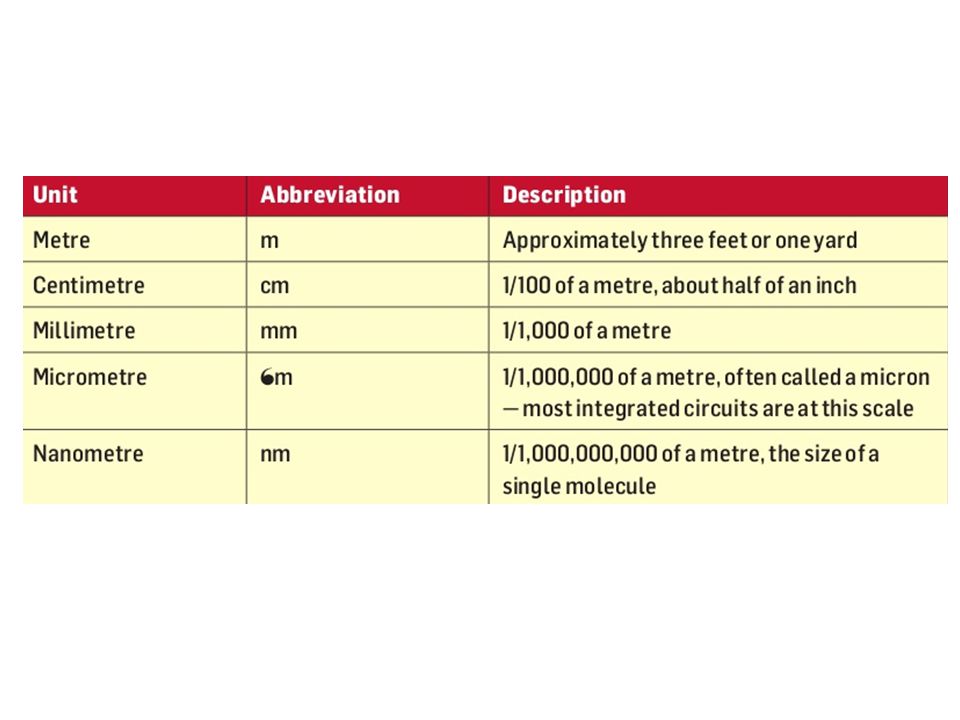
A nanometre (Greek: νάνος, nanos, "dwarf"; μέτρον, metrοn) is a unit of length in the metric system, equal to one billionth of a meter (i.e., 10-9 m or one millionth of a millimeter). Real world scenario: Humans are 10,000,000 times smaller than the earth. A 100 nm sized particle, is 10,000,000 times smaller than a human. Scaling down High surface area High payload Multi-functionality Low overall therapeutics/NP At scales on the order of 100’s of nm, novel materials properties emerge, enabling the development of new class of materials. It can create opportunities for paradigm shifting results, creating new preventive, diagnostic and therapeutic approaches to cancer 100 nm
 is a unit of length in the metric system, equal to one billionth of a meter (i.e., 10-9 m or one millionth of a millimeter). Real world scenario: Humans are 10,000,000 times smaller than the earth. A 100 nm sized particle, is 10,000,000 times smaller than a human. Scaling. down. High surface area. High payload. Multi-functionality. Low overall therapeutics/NP. At scales on the order of 100’s of nm, novel materials properties emerge, enabling the development of new class of materials. It can create opportunities for paradigm shifting results, creating new preventive, diagnostic and therapeutic approaches to cancer. 100 nm. ArticleID=1780.")
11
The Importance of Size What makes Nanotech unique? This is Star Trek stuff. It literally allows scientists and industry to build entirely new materials or machines that we may have only imagined in the past….but now, the limits of our imagination our being re-defined. WE CAN NOW REALLY THINK OUTSIDE THE BOX. Features: Small Particles- More surface area, more atoms to contact a surface Extremely precise – Materials can be made close to perfection to the point that exact number of atoms can be measured.

12
University of Illinois

13
What’s the BIG deal about something so SMALL?
Materials behave differently at this size scale. It’s not just about miniaturization. At this scale---it’s all about INTERFACES Color depends on particle size Quantum dots 3.2 nm in diameter have blue emission Quantum dots 5 nm in diameter have red emission

14
Working at the atomic, molecular and supra-molecular levels, in the length scale of approximately 1 – 100 nm range, through the control and manipulation of matter at the atomic and molecular level in order to design, create and use materials, devices and systems with fundamentally new properties and functions because of their small structure.

15
Why can’t we manipulate materials atom by atom?
Richard Feynman’s famous presentation “There’s Plenty of Room at the Bottom” was in the 1959 at the American Physical Society. Here he asked: Why can’t we manipulate materials atom by atom? Why can’t we control the synthesis of individual molecules? Why can’t we write all of human knowledge on the head of a pin? Why can’t we build machines to accomplish these things? Nobel Prize in Physics 1965

16
Nanotechnology: A Blast from Past?
How old is nanotechnology in human history? Lead sulfide crystals (5 nm) Blonde hair Silver nano-colloids were used by Persians, Babylonian and Greek civilizations as antiobiotics The astounding qualities of “nano”-gold were understood by the ancients, who devoted massive amounts of time and energy to alchemy and labeled a primitive form of Nanogold the “Elixir of Life.” It's over 4000 years old. Goes back in ancient Egyptian and Persian times
 Blonde hair. Silver nano-colloids were used by Persians, Babylonian and Greek civilizations as antiobiotics. The astounding qualities of nano -gold were understood by the ancients, who devoted massive amounts of time and energy to alchemy and labeled a primitive form of Nanogold the Elixir of Life. It s over 4000 years old. Goes back in ancient Egyptian and Persian times.")
17
History of Nanotechnology

18
Nanotechnology Through History: Carbon-based Nanoparticles from Prehistory to Today
17,000-year old cave paintings from the Lascaux caves in southwestern France. The pigment’s resemblance of soot is no accident.

19
The Oldest Nanoparticle in History
Since our early ancestors first learned to make fires, humans have been producing carbon-based nanoparticles. The smoke and soot from their campfires contained nanoparticles known as fullerenes and carbon nanotubes, along with many other combustion by-products. They must have thought the very crude nanoparticle preparations they created were a bit of a nuisance (depending on how concerned they were about cleanliness), until they decided they could use them in art. Little did they realize that some of the structures in the smudgy black stuff they made would some day help solve our energy problems.
, until they decided they could use them in art. Little did they realize that some of the structures in the smudgy black stuff they made would some day help solve our energy problems.")
20
Thousands of years later, in the 11th to 13th centuries C. E
Thousands of years later, in the 11th to 13th centuries C.E., the Crusaders encountered unusually strong and sharp sword blades when then fought against Muslims. Part of the reason for the exceptional strength, remarkable sharpness, and beautiful patterns on the surface of the Damascus steel sword blades used by Saladin’s troops may have been the presence of carbon nanotubes in the steel used. Scientists looking at such sword blades under the electron microscope have seen evidence of carbon nanotubes (and other nanomaterials) in Damascus steel.
 in Damascus steel.")
21
Why Now? New tools for atomic-scale characterization
New capabilities for single atom/molecule manipulation Computational access to large systems of atoms and long time scales Convergence of scientific-disciplines at the nanoscale

22
Technology Momentum Reminders
"There is no reason anyone would want a computer in their home." (Ken Olsen, Digital Equipment Corp, 1977) "Computers in the future may weigh no more than 1.5 tons." (Popular Mechanics, 1949) "I think there is a world market for maybe five computers." (IBM's Thomas Watson, 1943)
 Computers in the future may weigh no more than 1.5 tons. (Popular Mechanics, 1949) I think there is a world market for maybe five computers. (IBM s Thomas Watson, 1943)")
23
Nanotechnology: Applications

24
Nanotechnology Applications

25
Benefits of Nanotechnology
“The power of nanotechnology is rooted in its potential to transform and revolutionize multiple technology and industry sectors, including aerospace, agriculture, biotechnology, homeland security and national defense, energy, environmental improvement, information technology, medicine, and transportation. Discovery in some of these areas has advanced to the point where it is now possible to identify applications that will impact the world we live in.” -National Nanotechnology Initiative

26
Understanding the Challenges of the Nanoscale
There are many length and time scales that are important in nanotechnology. Length scale goes from 10 Å to 104 Å this corresponds to 102 to 1011 particles Time scales ranging from s to several seconds The temporal scale goes linearly in the number of particles N, the spatial scale goes as (NlogN), yet the accuracy scale can go as high as N7 to N! with a significant pre-factor.
, yet the accuracy scale can go as high as N7 to N! with a significant pre-factor.")
27
Challenges of this Size Scale
A critical issue for nanotechnology is that components, structures, and systems are in a size regime about whose fundamental behavior we have little understanding. They are: too small for direct measurements too large to be described by current rigorous first principle theoretical and computational methods exhibit too many fluctuations to be treated monolithically in time and space too few to be described by a statistical ensemble.

28
Nanoscience will change the nature of almost every human-made object in the next century.
National Science and Technology Council, 2000

29
Economic Impact of Nanotechnology
Market Size Predictions (within a decade)* $340B/yr Materials $300B/yr Electronics $180B/yr Pharmaceuticals $100B/yr Chemical manufacture $ 70B/yr Aerospace $ 20B/yr Tools $ 30B/yr Improved healthcare $ 45B/yr Sustainability $1 Trillion per year by 2015 *2007 Estimates by industry groups, source: NSF
* $340B/yr Materials. $300B/yr Electronics. $180B/yr Pharmaceuticals. $100B/yr Chemical manufacture. $ 70B/yr Aerospace. $ 20B/yr Tools. $ 30B/yr Improved healthcare. $ 45B/yr Sustainability. $1 Trillion per year by *2007 Estimates by industry groups, source: NSF.")
30
Economic Impact of Nanotechnology
According to “The Nanotechnology Opportunity Report (NOR),” 3rd Edition Cientifica Ltd., published in June 2008 “The market for products enabled by nano-technologies will reach US$ 263 billion by 2012.” “The highest growth rates will be in the convergence between bio- and nanotechnologies in the healthcare and pharmaceutical sectors.”
, 3rd Edition Cientifica Ltd., published in June The market for products enabled by nano-technologies will reach US$ 263 billion by The highest growth rates will be in the convergence between bio- and nanotechnologies in the healthcare and pharmaceutical sectors.")
31
National Investment Fiscal Year NNI 2000 $270M 2001 $464M 2002 $697M 2003 $862M 2004 $989M 2005 $1,200M 2006 $1,303M 2007 $1,425M 2008 $1,491M 2009 $1,527M The US investment in nano-technology represents about ¼ of the world R&D investment. The 2010 Budget provides $1.6 billion, reflecting steady growth in the NNI investment.

32
U.S Market Nanomaterials Projections
The US market for nanomaterials (which totaled only $125 million in 2000) is expected to surpass $1 billion in 2007 and reach $35 billion by Early growth will come from numerous niche applications that span the entire US manufacturing sector. These include wafer polishing abrasives and high density data storage media for the electronics industry; improved diagnostic aids for the medical community; transparent sunscreens, stain-resistant pants and wear-resistant flooring for consumers; cost-cutting equipment coatings for the defense industry; fuel-saving components for the auto industry; and better paper and ink for the printing industry. In the long run, however, the best opportunities are expected in health care and electronics, which together are expected to comprise nearly two-thirds of the market by 2020 Source: The Fredonia Group
 is expected to surpass $1 billion in 2007 and reach $35 billion by Early growth will come from numerous niche applications that span the entire US manufacturing sector. These include wafer polishing abrasives and high density data storage media for the electronics industry; improved diagnostic aids for the medical community; transparent sunscreens, stain-resistant pants and wear-resistant flooring for consumers; cost-cutting equipment coatings for the defense industry; fuel-saving components for the auto industry; and better paper and ink for the printing industry. In the long run, however, the best opportunities are expected in health care and electronics, which together are expected to comprise nearly two-thirds of the market by Source: The Fredonia Group.")
33
Examples of Current Research and Applications
Materials Science Powders, Coatings, Carbon Nano-Materials, C-NanoFabrics Energy Solar Power and PhotoVoltaics, Hydrogen Fuel Cells, LED White Light Medicine/Biotech Genomics, Proteomics, Lab on a Chip, C-Nanotubes, BuckyBalls Electronics MRAM, NRAM, Q-Dots, Q-Bits Devices Lithography, Dip Pen Lithography, AFM, MEMS A 64 qbit computer is roughly 18 Billion times as powerful as a 64 bit binary. What would take a Pentium class digital computer pulling 2 billion calculations per second to solve a 64 bit encryption key (292 years) a 64 Qbit computer could do it in one operation. Moore’s law is reaching its limit. Silicon based chips are predicted to hit their size limit by What now takes a MOSFET (metal oxide semiconductor field effect transistor 1000 electrons to switch on and off, quantum dot based SET’s can do with a single electron. Benefits- tens or hundreds of times more efficient and Much, much faster. IBM and Hewlett Packard Both will launch products late in 2003 that will give 40x’s more storage capacity than the most advanced chips in 2002.
 a 64 Qbit computer could do it in one operation. Moore’s law is reaching its limit. Silicon based chips are predicted to hit their size limit by What now takes a MOSFET (metal oxide semiconductor field effect transistor 1000 electrons to switch on and off, quantum dot based SET’s can do with a single electron. Benefits- tens or hundreds of times more efficient and Much, much faster. IBM and Hewlett Packard Both will launch products late in 2003 that will give 40x’s more storage capacity than the most advanced chips in")
34
Modeling, Characterization and Fabrication are Inseparable for Nanoscale Devices
Simulation Characterization Fabrication Applications Courtesy: NASA

35
Sporting Goods

36
Cosmetics, Clothes and Food

37
Clean and Cheap Energy Solid oxide fuel cell Computational catalysis
Courtesy: Steve McIntosh, UVA Computational catalysis Courtesy: Matthew Neurock, UVA Laser-textured silicon for solar cells Courtesy: Mool Gupta, UVA

38
Courtesy of NASA

39
Disruptive Apps - Materials
Fiber that is stronger than spider web Metal 100 x’s stronger than steel, 1/6 weight Catalysts that respond more quickly and to more agents Plastics that conduct electricity Coatings that are nearly frictionless –(Shipping Industry) Materials that change color and transparency on demand. Materials that are self repairing, self cleaning, and never need repainting. Nanoscale powders that are five times as light as plastic but provide the same radiation protection as metal. Examples – Clothing that can act as a computer, TV’s that use Carbon Nanotubes – vibrant pictures, from any angle, much thinner, use less energy. Flooring tiles that can never be scratched and change color or pattern on demand. Nanolubricants that can operate at much higher temperatures. Building tiles coated with Titanium Dioxide Nano Particles that never need repainting or washing (What happens to the 17b paint industry?) Refrig. And counter tops that clean themselves (what happens to paper towels and cleaning product companies?) Impermeable plastic beer bottles that don’t allow hydrogen to escape – allowing them to be stored much longer. (What happens to the overland shipping industry or beer distribution companies?) Car windows that can’t be broken, materials that fix themselves when dented – how does this impact insurance industry?
 Materials that change color and transparency on demand. Materials that are self repairing, self cleaning, and never need repainting. Nanoscale powders that are five times as light as plastic but provide the same radiation protection as metal. Examples – Clothing that can act as a computer, TV’s that use Carbon Nanotubes – vibrant pictures, from any angle, much thinner, use less energy. Flooring tiles that can never be scratched and change color or pattern on demand. Nanolubricants that can operate at much higher temperatures. Building tiles coated with Titanium Dioxide Nano Particles that never need repainting or washing (What happens to the 17b paint industry ) Refrig. And counter tops that clean themselves (what happens to paper towels and cleaning product companies ) Impermeable plastic beer bottles that don’t allow hydrogen to escape – allowing them to be stored much longer. (What happens to the overland shipping industry or beer distribution companies ) Car windows that can’t be broken, materials that fix themselves when dented – how does this impact insurance industry")
40
Disruptive Apps - Energy
Fuel cell technology becomes cost effective within 3 years. Batteries that store more energy and are much more efficient Plastics and paints that will store solar power and convert to energy for $1 per watt. Fuel Cells – Nanotech creates materials strong enough to withstand high pressure while containing very small hydrogen atoms. Nano membranes will more easily separate hydrogen from many sources,Graphite fibers will absorb more hydrogen by weight increasing storage capacity, nanocatalysts will split hydrogens more easily increasing power of each cell, new sensors can detect any leak before it becomes a threat. Toyota introduces a new fuel cell car in 2003 –but implications extend into entire energy sector. Batteries will begin to use Carbon Nanotubes instead of graphite, increasing storage and battery life – computers, cell phones, go longer before charging and changing the 10b. Battery market.

41
Disruptive Apps - Computing
Silicon is hitting its size limit, Moore’s law reaches maximum in 2007 SuperChips –Combination of Silicon and Galium Arsenide create wireless chips Plastic semiconductors manufactured by regular printing devices – cheaply produced. Electronic Paper With electronic paper – bright vivid images can be viewed on demand under any condition while still maintaining the look of regular paper. (what happens to the 108b printing industry and the 60b newspaper, 59b periodical, and 23b. Book industry?) It also is light, flexible, and fast download speeds. Electronic billboards will erode instore displays and highway signage. Prices change instantaneously, (Macy’s spends 250 k/week to change prices)
 It also is light, flexible, and fast download speeds. Electronic billboards will erode instore displays and highway signage. Prices change instantaneously, (Macy’s spends 250 k/week to change prices)")
42
Disruptive Apps – Bio Medicine
Cosmetics that can penetrate the skin Cures for Aids, Cancers, Alzheimer's, Diabetes Ability to view cells In vivo - Fast Drug Creation Nanomaterials that can see inside vessels for plaque buildup Technology that can re-grow bone and organs NanoSensors for disease detection – 10x’s faster and 100,000 x’s more accurate Nano filters will help create impurity free drugs If Alzheimers is cured, how will that impact the elderly care industry? If diabetes can be automatically controlled with nanodevices, how will that impact the food industry? Health Insurance Industry? New estrogen lotion using nanoparticles that penetrates skin – could replace premarin, 3rd most prescribed drug in America. Nanoscale Materials Inc. has produced a skin cream that provides instant protection against anthrax and another that is sprayed from fire extinguisher to render Anthrax harmless. Nanosensors that can test immediately for hundreds and even thousands of viruses simultaneously – (what happens to companies that specialize in testing for disease, lab technicians, suppliers of these labs?) Radioactive smart bombs with Buckyballs – radioactive actinium 225 atom is placed inside, protein on the outside, protein attaches only to the cancer cell.
 Radioactive smart bombs with Buckyballs – radioactive actinium 225 atom is placed inside, protein on the outside, protein attaches only to the cancer cell.")
43
Definition A particle having one or more dimensions of the order of 100nm (10-7 m) or less From 101nm 101nm 96nm 116nm 154nm 201nm

44
Taking Inspiration from Mother Nature
Gecko feet are covered with nano-size hairs that use intermolecular forces, allowing the lizards to stick firmly to surfaces. By replicating this scientists have developed an adhesive that can seal wounds or patch a hole caused by a stomach ulcer. The adhesive is elastic, waterproof and made of material that breaks down as the injury heals.

45
Key Terms You Need to Know
BuckyBalls Carbon Nanotubes MEMS Quantum Dots Molecular Self Repair/Assembly MRAM/Spintronics Lithography Metal nanoparticles Imaging Therapy

46
Carbon Nanotubes 4 nm width (smaller diameter than DNA)
100x’s stronger than steel 1/6 weight Thermal/electrically conductive Metallic and Semi-Conductive Carbon Nanotube. Strong covalent bonding, unique one-dimensional structure and nanometer size, together impart unusual properties to the nanotubes. These properties include exceptionally high tensile strength, high resilience, electronic properties ranging from metallic to semi-conducting, the ability to sustain high current densities and high thermal conductivity. Thus carbon nanotubes could be used as fillers in super-strong composite materials, as wires and components in nano-electronic devices, as tips of scanning probe microscopes and in flat panel displays and gas sensors. Our vision for the field has been in place for some time: “…if the [single-walled carbon nanotubes] SWNTs are to achieve their full potential, it will be necessary to bring about chemical modification of the basic structure. The ability to disperse and perhaps dissolve the SWNTs would greatly improve the prospects for processable materials that can be aligned and formed into useful structures. Chemical functionalization would be an important step in this direction as well as opening up interesting opportunities in its own right. If it were possible to chemically modify the surface of the nanotubes in a controlled manner, this would afford a number of opportunities for tailoring the structural and electronic properties.”[1,2] At full size, we view carbon nanotubes as macromolecules that should be ideal constituents of polymers, copolymers, polymer composites, and biological structures where their outstanding physical properties, such as high strength, exceptional thermal conductivity, and singular electronic properties distinguish them from all other nanomaterials.[3] The carbon nanotube is the ultimate molecular carbon fiber – if it can be processed into useful structures. At the other end of the size scale, where the nanotubes are shortened to the molecular size regime,[4] interest will focus on their unique cylindrical physical shape together with their conjugated electronic structure. While the chemistry of nanotubes is in its infancy, considerable progress can be noted. The dissolution of SWNTs in common organic solvents has been demonstrated,[5-7] as has end-group[4-8] and side-wall[5,9] chemistry. The issues that face the nascent carbon nanotube industry are frequently underestimated in the scientific literature and the press releases. Nanotubes still cost much more than gold on a weight basis, most preparations are highly impure and many of the purifications reported in the literature do not work as stated. Purification of the carbon nanotubes is a particular problem in the case of the electric arc and laser oven-produced materials due to the occurrence of nanoparticles. Cross flow filtration[4,10] probably remains the technique of choice for these production methods, but the procedure is labor intensive and difficult to scale to large batch sizes. In general, the purification methods are rather specific for the particular type of carbon nanotube that is to be processed.[11] Chromatographic methods have given pure materials, but the prospects of scaling up these procedures are not encouraging.[12-17] ***Fluorinating nanotubes also makes it easier for scientists and engineers to exploit their incredible strength. SWNTs are 100 times stronger then steel at one-sixth the weight. With their tendency to clump together, though, engineers haven't been able to use them effectively in creating superstrong composite materials. Research by Margrave and others at Rice has shown that disentangling SWNTs via fluorination makes it easier to disperse them evenly in polymers and ceramic composites.

47
BuckyBalls – C60 Roundest and most symmetrical molecule known to man
Compressed – becomes stronger than diamond Third major form of pure carbon Heat resistance and electrical conductivity Bucky Ball: "It is the roundest and most symmetrical large molecule known to man. Buckministerfullerine continues to astonish with one amazing property after another. Named after American architect R. Buckminister Fuller who designed a geodesic dome with the same fundamental symmetry, C60 is the third major form of pure carbon; graphite and diamond are the other two." Bucky Balls - Andy Gion. AKA: C60 molecules & buckminsterfullerene. Molecules made up of 60 carbon atoms arranged in a series of interlocking hexagons and pentagons, forming a structure that looks similar to a soccer ball [Steffen Weber, PhD.]. C60 is actually a "truncated icosahedron", consisting of 12 pentagons and 20 hexagons. It was discovered in 1985 by Professor Sir Harry Kroto, and two Rice University professors, chemists Dr. Richard E. Smalley and Dr. Robert F. Curl Jr., [for which they were jointly awarded the 1996 Nobel Lauriate for chemistry] and is the only molecule composed of a single element to form a hollow spheroid [which gives the potential for filling it, and using it for novel drug-delivery systems. See Structure of a New Family of Buckyballs Created]. "The buckyball, being the roundest of round molecules, is also quite resistant to high speed collisions. In fact, the buckyball can withstand slamming into a stainless steel plate at 15,000 mph, merely bouncing back, unharmed. When compressed to 70 percent of its original size, the buckyball becomes more than twice as hard as its cousin, diamond." The Buckyball - Rodrigo de Almeida Siqueira. Because the buckyballs sphere is hollow, other atoms can be trapped within it. The have heat-resistance and electrical conductivity. Their applications appear to be endless. Current research indicates that some of their projected applications are: „X Polymers/reinforcements „X Compounds „X High quality diamond films for electronic chips and other devices. „X Insulator „X Batteries and fuel cell electrodes „X Strengthening and hardening of metals „X Sensor applications „X Surface hardening coatings „X Catalysts „X Biological/pharmaceuticals „X Copier toner „X Organic chemistry building blocks „X Chemical reagents

48
MEMS and Quantum Dots Micro Sized Motor Quantum Dot
MEMS is also not about making things out of silicon, even though silicon possesses excellent materials properties, which make it an attractive choice for many high-performance mechanical applications; for example, the strength-to-weight ratio for silicon is higher than many other engineering materials which allows very high-bandwidth mechanical devices to be realized. Instead, the deep insight of MEMS is as a new manufacturing technology, a way of making complex electromechanical systems using batch fabrication techniques similar to those used for integrated circuits, and uniting these electromechanical elements together with electronics. Advantages of MEMS Manufacturing First, MEMS is an extremely diverse technology that could significantly affect every category of commercial and military product. MEMS are already used for tasks ranging from in-dwelling blood pressure monitoring to active suspension systems for automobiles. The nature of MEMS technology and its diversity of useful applications make it potentially a far more pervasive technology than even integrated circuit microchips. Second, MEMS blurs the distinction between complex mechanical systems and integrated circuit electronics. Historically, sensors and actuators are the most costly and unreliable part of a macroscale sensor-actuator-electronics system. MEMS technology allows these complex electromechanical systems to be manufactured using batch fabrication techniques, increasing the reliability of the sensors and actuators to equal that of integrated circuits. Yet, even though the performance of MEMS devices and systems is expected to be superior to macroscale components and systems, the price is predicted to be much lower.

49
Obstacles and Hurdles Mass Production/Throughput and Cost Constraints
Safety- Unknown Regulatory Issues Funding Requires Long-Term Investments Intellectual Property Issues - Patent Office that is Overwhelmed and Under-Qualified The issues that face the nascent carbon nanotube industry are frequently underestimated in the scientific literature and the press releases. Nanotubes still cost much more than gold on a weight basis, most preparations are highly impure and many of the purifications reported in the literature do not work as stated. Purification of the carbon nanotubes is a particular problem in the case of the electric arc and laser oven-produced materials due to the occurrence of nanoparticles. Cross flow filtration[4,10] probably remains the technique of choice for these production methods, but the procedure is labor intensive and difficult to scale to large batch sizes. In general, the purification methods are rather specific for the particular type of carbon nanotube that is to be processed.[11] Chromatographic methods have given pure materials, but the prospects of scaling up these procedures are not encouraging

50
Resources Must Read Books As the Future Catches You – Juan Enriquez
Investors Guide to Nanotechnology and Micromachines – Glenn Fishbine Next Big Thing Is Really Small: How Nanotechnology Will Change the Future of Your Business – Jack Uldrich, Deb Newberry Hacking Matter – Will McCarthey Periodicals Forbes/Wolfe Nanotech Report MIT Technology Review Science Nature Web –

51
References An inventory of nanotechnology-based consumer products currently on the market. Productive Nanosystems A Technology Roadmap, 2007, Battelle Memorial Institute and Foresight Nanotech Institute. IWGN Workshop Report: Nanotechnology Research Directions: Vision for Nanotechnology in the Next Decade, 2000, Edited by M.C. Roco, R.S. Williams, and P. Alivisatos, Springer.

Similar presentations


![L 33 Modern Physics [1] Introduction- quantum physics Particles of light PHOTONS The photoelectric effect –Photocells & intrusion detection devices The.](/19/5723857/big_thumb.jpg "L 33 Modern Physics [1] Introduction- quantum physics Particles of light PHOTONS The photoelectric effect –Photocells & intrusion detection devices The.>")


