Download presentation
Presentation is loading. Please wait.

1
YoHan Kim 0540541

4
Thin Film Layer of material ranging from fractions of nanometer to several micro meters in thickness Thin Film Process Process to make thin film on a substrate

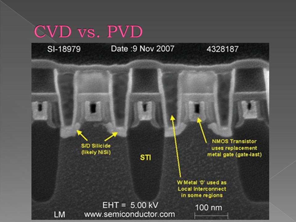
5
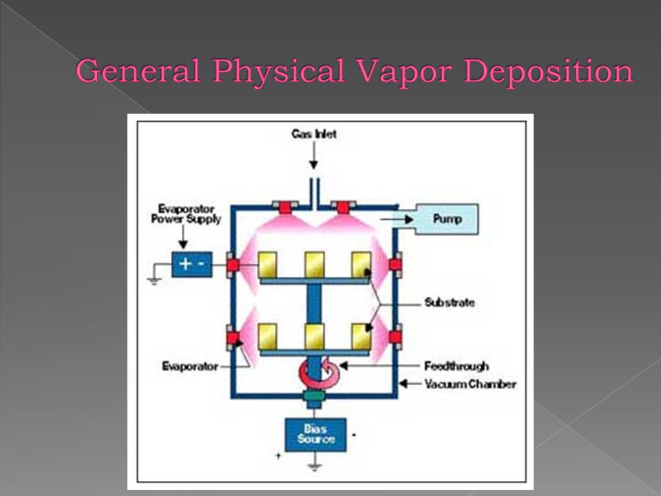
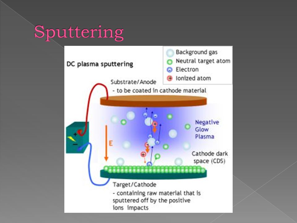
Thermal oxidation Physical Vapor Deposition Vaporized material bombards onto substrate, i.e. Si wafer. Chemical Vapor Deposition Gaseous material reacts on substrate to form thin film

6
Vacuum deposition Evaporation of material required More expensive, but high quality Sputtering is widely used Aluminum, Titanium, Titanium nitrate, Tungsten silicide

9
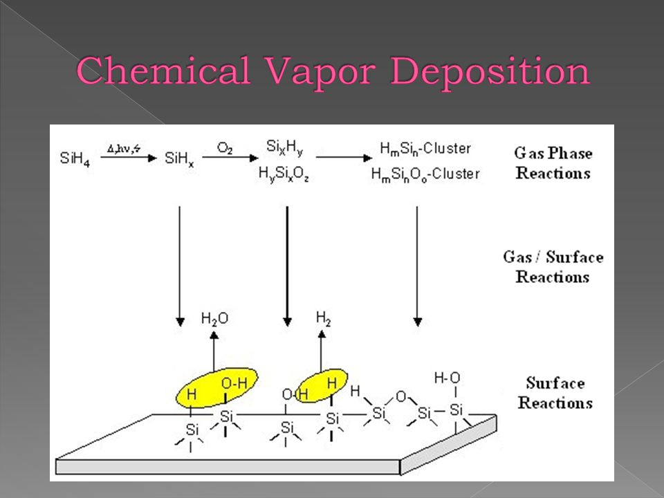
Gas form of material goes under chemical reaction with substrate to form thin film Remnant gas remains after reaction Fast, cheap, but poor quality Forms variety of thin film

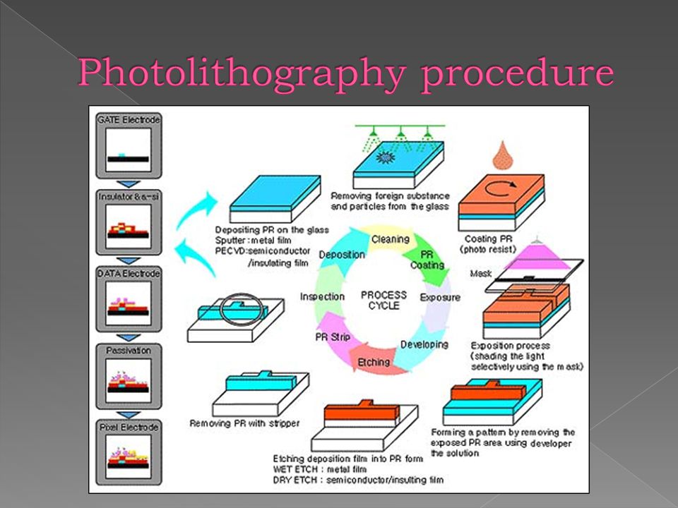
12
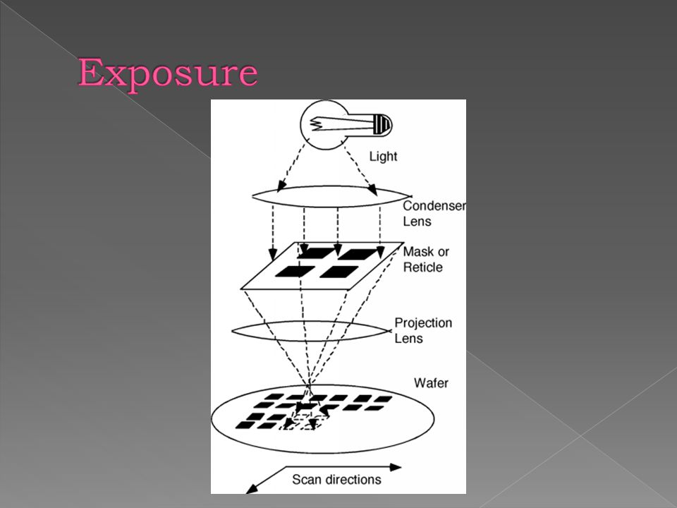
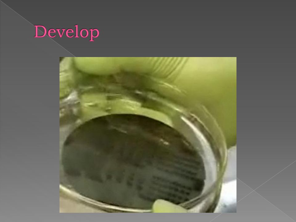
Process to make patterns on a wafer Removes unwanted area of thin film deposited in previous stage

14
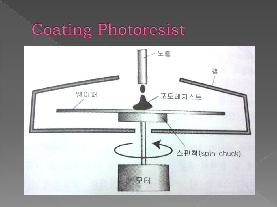
Key of Photolithography, called PR Type of organic material Very sensitive to UV

15
Two types of photoresist Positive: Exposed PR is removed Negative: Exposed PR remains

19
Wet Etching uses chemicals Dry Etching uses plasma

20
Photoresist is organic material Must be stripped off after etching

21
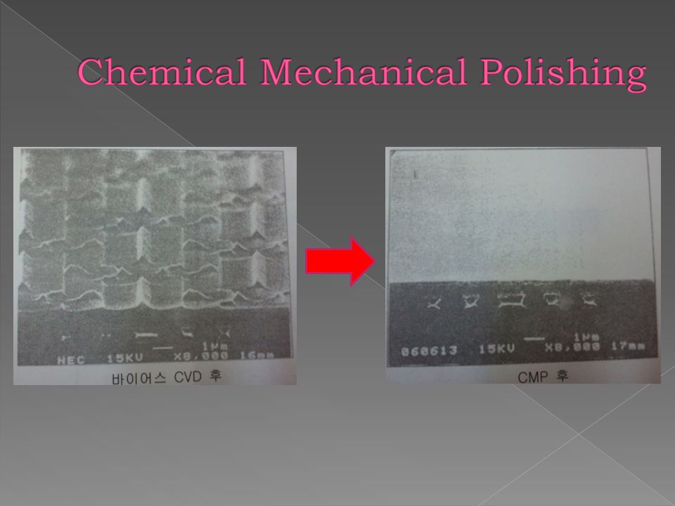
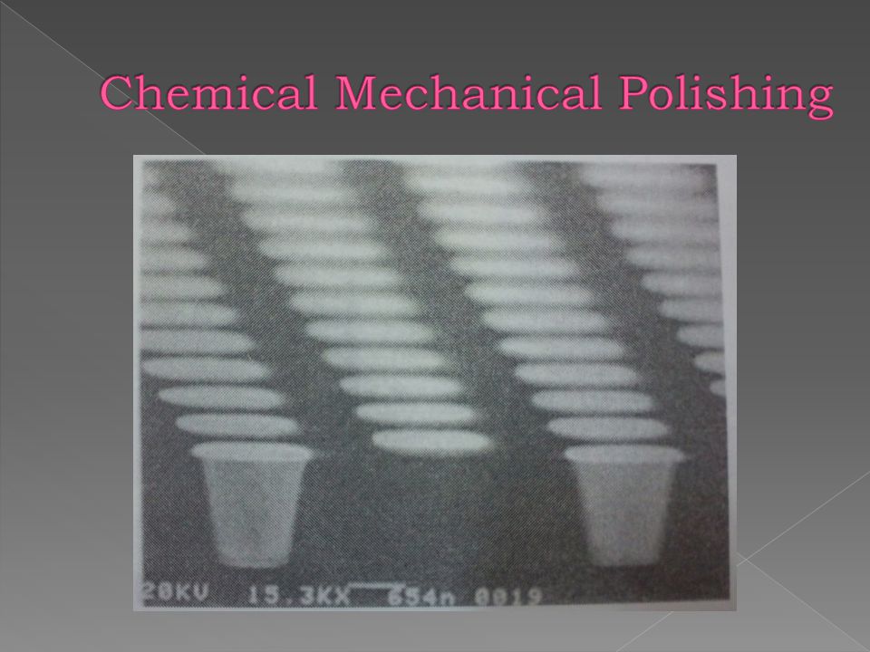
Sometimes the surface has to be flattened after removing PR Mechanically polished

24
Fabricating nanoscale device is repetition of thin film process and photolithography Up to 20~30 cycles are repeated Each layer of semiconductor requires at least 2 photolithography masks

25
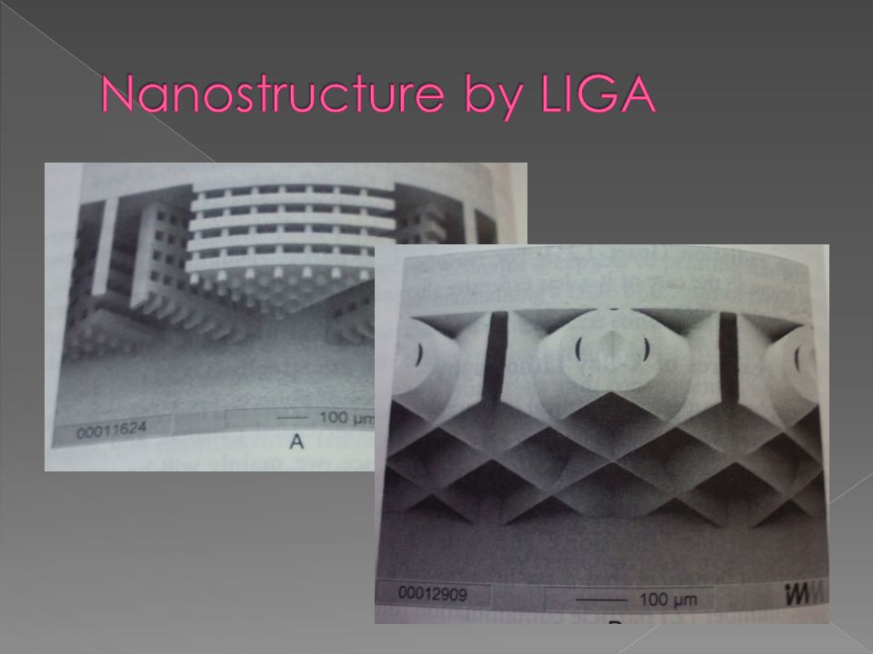
Extreme UV lithography X-Ray Lithography LIGA(x-ray lithographie galvanoformung abformtechnik), German acronym which means “x-ray lithography electro- deposition moding LIGA is good in 3D fabrication Photolithography will not be abandoned
, German acronym which means x-ray lithography electro- deposition moding LIGA is good in 3D fabrication Photolithography will not be abandoned")
Similar presentations


>")


 Grey=Si, Blue=Silicon Dioxide, Red=Photoresist, Purple= Phosphorus.>")


![Fabrication of p-n junction in Si Silicon wafer [1-0-0] Type: N Dopant: P Resistivity: 10-20 Ω-cm Thickness: 505-545 µm.](/15/4784305/big_thumb.jpg "Fabrication of p-n junction in Si Silicon wafer [1-0-0] Type: N Dopant: P Resistivity: 10-20 Ω-cm Thickness: 505-545 µm.>")


>")


