Download presentation
Presentation is loading. Please wait.

1
EDA 實作 Verilog Tutorial 國研院國家晶片系統設計中心 July 2005 陳正斌

2
Traditional VLSI Design Flow

4
EDA Electronic Design Automation (EDA) Computer-Aided Design (CAD)
 Computer-Aided Design (CAD)")
5
Hardware Description Language A hardware description language (HDL) is a high- level programming language with special constructs used to model the function of hardware logic circuits. The special language constructs can: –Describe the connectivity of the circuit –Describe the functionality of the circuit –Describe the timing of a circuit

6
Verilog Verilog is a Hardware Description Language. Verilog models digital circuits. Verilog lets you develop tests to verify the functionality of the circuits you model.

7
Verilog Module

8
Module Ports

9
Module Instances

10
A Simple and Complete Example

11
Sample Design – Full Adder x in y in c in coutsum 00000 00101 01001 01110 10001 10110 11010 11111

12
Full Adder – Boolean Algebra cout = x in y in c in ’+ x in y in c in +x in ’y in c in +x in y in ’c in = x in y in +c in (x in ’y in +x in y in ’) = x in y in + c in (x in ⊕ y in ) sum = x in ’y in ’c in + x in ’y in c in ’+x in y in ’c in ’+x in y in c in = (x in ’y in +x in y in ’)c in ’ + (x in ’y in ’+x in y in ) c in = (x in ⊕ y in ) ⊕ c in
 = x in y in + c in (x in ⊕ y in ) sum = x in ’y in ’c in + x in ’y in c in ’+x in y in ’c in ’+x in y in c in = (x in ’y in +x in y in ’)c in ’ + (x in ’y in ’+x in y in ) c in = (x in ⊕ y in ) ⊕ c in")
13
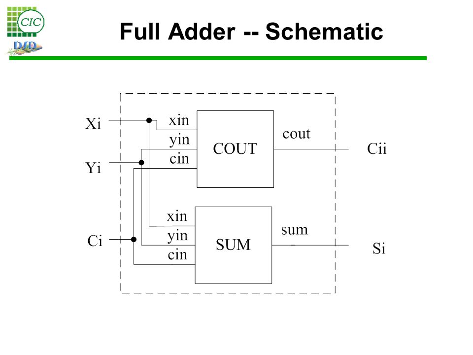
Full Adder – Schematic

14
Full Adder – Verilog Model module COUT(cout, xin, yin, cin); input xin; input yin; input cin; output cout; wire xin, yin, cin, out; wire p1, p2, p3; and (p1, xin, yin); xor (p2, xin, yin); and (p3, p2, cin); or (cout, p1, p3); endmodule module SUM(sum, xin, yin, cin); input xin; input yin; input cin; output sum; xor (sum, xin, yin, cin); endmodule
; input xin; input yin; input cin; output cout; wire xin, yin, cin, out; wire p1, p2, p3; and (p1, xin, yin); xor (p2, xin, yin); and (p3, p2, cin); or (cout, p1, p3); endmodule module SUM(sum, xin, yin, cin); input xin; input yin; input cin; output sum; xor (sum, xin, yin, cin); endmodule")
15
Full Adder -- Schematic

17
Full Adder – Verilog Model module FA(Cii,Si,Xi,Yi,Ci); input Xi; input Yi; input Ci; output Cii; output Si; SUM inst0 (.sum(Si),.xin(Xi),.yin(Yi),.cin(Ci)); COUT inst1 (.cout(Cii),.xin(Xi),.yin(Yi),.cin(Ci)); endmodule
; input Xi; input Yi; input Ci; output Cii; output Si; SUM inst0 (.sum(Si),.xin(Xi),.yin(Yi),.cin(Ci)); COUT inst1 (.cout(Cii),.xin(Xi),.yin(Yi),.cin(Ci)); endmodule")
18
Test Bench -- Template module FA_test; //Signal declaration //Instantiate modules //Apply stimulus //Display results endmodule

19
Test Bench --Instance module FA_test; //Signal declaration //Instantiate modules FA inst0 (Cii,Si,Xi,Yi,Ci); //Apply stimulus //Display results endmodule
; //Apply stimulus //Display results endmodule")
20
Test Bench -- Stimulus module FA_test; // Signal declaration reg Xi, Yi, Ci; // Instantiate modules FA inst0 (Cii,Si,Xi,Yi,Ci); // Apply Stimulus initial begin #0 Xi = 0; Yi = 0; Ci = 0; #10 Xi = 0; Yi = 0; Ci = 1; #10 Xi = 0; Yi = 1; Ci = 0; #10 Xi = 0; Yi = 1; Ci = 1; #10 $finish; end //Display results endmodule TimeValues XiYiCi 0000 10001 20010 30011
; // Apply Stimulus initial begin #0 Xi = 0; Yi = 0; Ci = 0; #10 Xi = 0; Yi = 0; Ci = 1; #10 Xi = 0; Yi = 1; Ci = 0; #10 Xi = 0; Yi = 1; Ci = 1; #10 $finish; end //Display results endmodule TimeValues XiYiCi")
21
Test Bench – Display Result module FA_test; // Signal declaration reg Xi, Yi, Ci; // Instantiate modules FA inst0 (Cii,Si,Xi,Yi,Ci); // Apply Stimulus initial begin #10 Xi = 0; Yi = 0; Ci = 0; #10 Xi = 0; Yi = 0; Ci = 1; #10 Xi = 0; Yi = 1; Ci = 0; #10 Xi = 0; Yi = 1; Ci = 1; #10 $finish; end //Display results initial // print all changes to all signal values $monitor($time, " Xi = %b Yi = %b Ci = %b Ci+1 = %b Si = %b", Xi,Yi,Ci,Cii,Si); endmodule
; // Apply Stimulus initial begin #10 Xi = 0; Yi = 0; Ci = 0; #10 Xi = 0; Yi = 0; Ci = 1; #10 Xi = 0; Yi = 1; Ci = 0; #10 Xi = 0; Yi = 1; Ci = 1; #10 $finish; end //Display results initial // print all changes to all signal values $monitor($time, Xi = %b Yi = %b Ci = %b Ci+1 = %b Si = %b , Xi,Yi,Ci,Cii,Si); endmodule")
22
Dump Waveform initial begin $dumpfile(“file.vcd”); $dumpvars(0,inst0); end
; $dumpvars(0,inst0); end")
23
Simulation unix> verilog FA_test.v FA.v COUT.v SUM.v unix> nWave &

24
Waveform

25
Quiz Design a 4 bit adder by instancing 4 full adder

26
Edit ADDR4.v module ADDR4(cout,sum,a,b,cin); input cin; input [3:0] a; input [3:0] b; output [3:0] sum; output cout; //Design Started Here!!! endmodule
![Edit ADDR4.v module ADDR4(cout,sum,a,b,cin); input cin; input [3:0] a; input [3:0] b; output [3:0] sum; output cout; //Design Started Here!!.](http://images.slideplayer.com/16/5050997/slides/slide_26.jpg "endmodule.")
27
Apply Stimulus Edit ADDR4_test.v // Apply Stimulus initial begin // ** Add stimulus here ** end

28
Apply Stimulus TimeValues abCin 0000 10351 2010110 30571 4015 0 5015 1 601510 701151 80780 905101 100490 110861 1207130 1309120 14014131

Similar presentations

 Set up basic environment Select Gates or Modules to Be simulated (Insert Program Code) Run Waveform.>")
; input.>")


 VHDL >")
 HDL Widely used in logic design Describe hardware Document logic functions.>")
 – e.g. VHDL/Verilog 2.Gate Level Design 3.Circuit Level.>")
? –A high-level computer language can model, represent.>")
