Download presentation
Presentation is loading. Please wait.

1
1 Introduction Chapters 2 & 3: Introduced increasingly complex digital building blocks –Gates, multiplexors, decoders, basic registers, and controllers Controllers good for systems with control inputs/outputs –Control input: Single bit (or just a few), representing environment event or state e.g., 1 bit representing button pressed –Data input: Multiple bits collectively representing single entity e.g., 7 bits representing temperature in binary Need building blocks for data –Datapath components, aka register-transfer-level (RTL) components, store/transform data Put datapath components together to form a datapath This chapter introduces numerous datapath components, and simple datapaths –Next chapter will combine controllers and datapaths into “processors” si z e ansis
, representing environment event or state e.g., 1 bit representing button pressed –Data input: Multiple bits collectively representing single entity e.g., 7 bits representing temperature in binary Need building blocks for data –Datapath components, aka register-transfer-level (RTL) components, store/transform data Put datapath components together to form a datapath This chapter introduces numerous datapath components, and simple datapaths –Next chapter will combine controllers and datapaths into processors si z e ansis")
2
2 Registers Can store data, very common in datapaths Basic register of Ch 3: Loaded every cycle –Useful for implementing FSM -- stores encoded state –For other uses, may want to load only on certain cycles si z e ansis Combinational logic State register s1s0 n1 n0 x b clk Basic register loads on every clock cycle load How extend to only load on certain cycles? a D Q D Q D Q D Q I2I3 Q2Q3Q1Q0 I1I0 clk 4-bit register

3
3 Register with Parallel Load Add 2x1 mux to front of each flip-flop Register’s load input selects mux input to pass –Either existing flip-flop value, or new value to load

4
4 Register Example using the Load Input: Weight Sampler Scale has two displays –Present weight –Saved weight –Useful to compare present item with previous item Use register to store weight –Pressing button causes present weight to be stored in register Register contents always displayed as “Saved weight,” even when new present weight appears Scale Saved weight Weight Sampler Present weight clk b Save I3I2I1I0 Q3Q2Q1Q0 load 3 pounds 0011 0011 0010 2 pounds 1 a

5
5 Shift Register Shift right –Move each bit one position right –Shift in 0 to leftmost bit 1 1 0 1 Register contents before shift right 0 1 1 0 0 Register contents after shift right a Q: Do four right shifts on 1001, showing value after each shift a A: 1001 (original) 0100 0010 0001 0000 shr_in Implementation: Connect flip-flop output to next flip-flop’s input a
 shr_in Implementation: Connect flip-flop output to next flip-flop’s input a")
6
6 Shift Register To allow register to either shift or retain, use 2x1 muxes –shr: 0 means retain, 1 shift –shr_in: value to shift in May be 0, or 1 Note: Can easily design shift register that shifts left instead

7
7 Multifunction Registers Many registers have multiple functions –Load, shift, clear (load all 0s) –And retain present value, of course Easily designed using muxes –Just connect each mux input to achieve desired function Functions: Operation Maintain present value Parallel load Shift right (unused - let's load 0s) s0 0 1 0 1 s1 0 0 1 1
 –And retain present value, of course Easily designed using muxes –Just connect each mux input to achieve desired function Functions: Operation Maintain present value Parallel load Shift right (unused - let s load 0s) s s")
8
8 Multifunction Registers Operation Maintain present value Parallel load Shift right Shift left s0 0 1 0 1 s1 0 0 1 1

9
9 Maintain value Shift left Shift right Parallel load Note Operation s0s1 0 1 1 1 0 0 0 0 0 1 0 0 1 1 1 1 OutputsInputs 0 1 0 1 0 1 0 1 0 0 1 1 0 0 1 1 0 0 0 0 1 1 1 1 ld shrshl Truth table for combinational circuit Multifunction Registers with Separate Control Inputs Maintain present value Shift left Shift right Shift right – shr has priority over shl Parallel load Parallel load – ld has priority Operationshlshrld 0 0 0 0 1 1 1 1 0 0 1 1 0 0 1 1 0 1 0 1 0 1 0 1 Q2Q1Q0Q3 Q2Q1Q0Q3 I2I1I0I3 I2I1I0I3 s1 shr_in shr shl ld s0 shl_in a a ? combi- national circuit a s1 = ld’*shr’*shl + ld’*shr*shl’ + ld’*shr*shl s0 = ld’*shr’*shl + ld

10
10 Register Operation Table Register operations typically shown using compact version of table –X means same operation whether value is 0 or 1 One X expands to two rows Two Xs expand to four rows –Put highest priority control input on left to make reduced table simple Maintain value Shift left Note Operation s0s1 0 1 0 1 OutputsInputs 0 1 0 0 0 0 Shift right 1 1 0 0 0 1 1 1 0 0 Parallel load 0 0 0 0 1 1 1 1 0 1 0 1 0 0 1 1 1 1 1 1 ld shrshl Maintainvalue Shift left Operationldshrshl 0 1 0 0 0 0 Parallel load XX1 Shift right X10

11
11 Register Design Process Can design register with desired operations using simple four-step process

12
12 Register Design Example Desired register operations –Load, shift left, synchronous clear, synchronous set Step 1: Determine mux size 5 operations: above, plus maintain present value (don’t forget this one!) --> Use 8x1 mux Step 2: Create mux operation table Step 3: Connect mux inputs Step 4: Map control lines Operation Maintain present value Parallel load Shift left Synchronous clear Synchronous set Maintain present value s0 0 1 0 1 0 1 0 1 s1 0 0 1 1 0 0 1 1 s2 0 0 0 0 1 1 1 1 D Q Qn 76321 In 054 10 s2 s1 s0 from Qn-1 Operation Maintain present value Shift left Parallel load Set to all 1s Clear to all 0s s0 0 0 1 0 1 s1 0 1 0 0 1 s2 0 0 0 1 0 shl 0 1 X X X ld 0 0 1 X X clr 0 0 0 0 1 InputsOutputs set 0 0 0 1 X a a s2 = clr’*set s1 = clr’*set’*ld’*shl + clr s0 = clr’*set’*ld + clr
 --> Use 8x1 mux Step 2: Create mux operation table Step 3: Connect mux inputs Step 4: Map control lines Operation Maintain present value Parallel load Shift left Synchronous clear Synchronous set Maintain present value s s s D Q Qn In s2 s1 s0 from Qn-1 Operation Maintain present value Shift left Parallel load Set to all 1s Clear to all 0s s s s shl 0 1 X X X ld X X clr InputsOutputs set X a a s2 = clr’*set s1 = clr’*set’*ld’*shl + clr s0 = clr’*set’*ld + clr")
13
13 Register Design Example Step 4: Map control lines Operation Maintain present value Shift left Parallel load Set to all 1s Clear to all 0s s0 0 0 1 0 1 s1 0 1 0 0 1 s2 0 0 0 1 0 shl 0 1 X X X ld 0 0 1 X X clr 0 0 0 0 1 InputsOutputs set 0 0 0 1 X s2 = clr’*set s1 = clr’*set’*ld’*shl + clr s0 = clr’*set’*ld + clr Q2Q1Q0Q3 Q2Q1Q0Q3 I2I1I0I3 I2I1I0I3 s1 ld shl s0 shl_in combi- national circuit set clr s2

14
14 Adders Adds two N-bit binary numbers –2-bit adder: adds two 2-bit numbers, outputs 3-bit result –e.g., 01 + 11 = 100 (1 + 3 = 4) Can design using combinational design process of Ch 2, but doesn’t work well for reasonable-size N –Why not? 0 1 0 1 1 0 1 0 1 1 0 0 1 0 0 1 0 0 1 1 0 1 1 1 0 1 0 1 0 1 0 1 0 0 1 1 0 0 1 1 1 1 1 1 1 1 1 1 0 0 0 0 1 1 1 1 s0 0 1 0 1 1 0 1 0 s1 0 0 1 1 0 1 1 0 c 0 0 0 0 0 0 0 1 b0 0 1 0 1 0 1 0 1 b1 0 0 1 1 0 0 1 1 a1 0 0 0 0 0 0 0 0 InputsOutputs a0 0 0 0 0 1 1 1 1

15
15 Why Adders Aren’t Built Using Standard Combinational Design Process Truth table too big –2-bit adder’s truth table shown Has 2 (2+2) = 16 rows –8-bit adder: 2 (8+8) = 65,536 rows –16-bit adder: 2 (16+16) = ~4 billion rows –32-bit adder:... Big truth table with numerous 1s/0s yields big logic –Plot shows number of transistors for N-bit adders, using state-of-the-art automated combinational design tool 0 1 0 1 1 0 1 0 1 1 0 0 1 0 0 1 0 0 1 1 0 1 1 1 0 1 0 1 0 1 0 1 0 0 1 1 0 0 1 1 1 1 1 1 1 1 1 1 0 0 0 0 1 1 1 1 s0 0 1 0 1 1 0 1 0 s1 0 0 1 1 0 1 1 0 c 0 0 0 0 0 0 0 1 b0 0 1 0 1 0 1 0 1 b1 0 0 1 1 0 0 1 1 a1 0 0 0 0 0 0 0 0 InputsOutputs a0 0 0 0 0 1 1 1 1 Q: Predict number of transistors for 16-bit adder A: 1000 transistors for N=5, doubles for each increase of N. So transistors = 1000*2 (N-5). Thus, for N=16, transistors = 1000*2 (16-5) = 1000*2048 = 2,048,000. Way too many! a 10000 8000 6000 4000 2000 0 12345 N 678 T r ansis t ors Transistors
. Thus, for N=16, transistors = 1000*2 (16-5) = 1000*2048 = 2,048,000. Way too many. a N 678 T r ansis t ors Transistors.")
16
16 Alternative Method to Design an Adder: Imitate Adding by Hand Alternative adder design: mimic how people do addition by hand One column at a time –Compute sum, add carry to next column 1 1 10 + 0 1 1 0 01 1 1 101 + 0 1 1 0 11 1 1 101 + 0 1 1 0 1 01 1 1 + 0 1 1 0 0 1 A: B: a

17
17 Alternative Method to Design an Adder: Imitate Adding by Hand Create component for each column –Adds that column’s bits, generates sum and carry bits 0 1 1 + 0 1 1 0 1 101 01 b cos 0 aci A: B: + 0 1 111 1 b cos 1 aci 1 b cos 0 a 1 110 b cos 1SUM a 0 A: B: 1 Half-adder Full-adders a

18
18 Half-Adder Half-adder: Adds 2 bits, generates sum and carry Design using combinational design process from Ch 2 b cos 0 aci A: B: + 0 1 111 1 1 b cos 1 aci 1 1 b cos 0 a 1 0 b cos 1SUM a 0 s 0 1 1 0 co 0 0 0 1 b 0 1 0 1 a 0 0 1 1 InputsOutputs Step 1: Capture the function Step 2: Convert to equations Step 3: Create the circuit co = ab s = a’b + ab’ (same as s = a xor b) ab co cos ab s Half-adder
 ab co cos ab s Half-adder")
19
19 Full-Adder Full-adder: Adds 3 bits, generates sum and carry Design using combinational design process from Ch 2 b cos 0 aci A: B: + 0 1 111 1 1 b cos 1 aci 1 1 b cos 0 a 1 0 b cos 1SUM a 0 Step 1: Capture the function s 0 1 1 0 1 0 0 1 co 0 0 0 1 0 1 1 1 ci 0 1 0 1 0 1 0 1 b 0 0 1 1 0 0 1 1 a 0 0 0 0 1 1 1 1 InputsOutputs Step 2: Convert to equations co = a’bc + ab’c + abc’ + abc co = a’bc +abc +ab’c +abc +abc’ +abc co = (a’+a)bc + (b’+b)ac + (c’+c)ab co = bc + ac + ab s = a’b’c + a’bc’ + ab’c’ + abc s = a’(b’c + bc’) + a(b’c’ + bc) s = a’(b xor c)’ + a(b xor c) s = a xor b xor c Step 3: Create the circuit co ciba s Full adder
bc + (b’+b)ac + (c’+c)ab co = bc + ac + ab s = a’b’c + a’bc’ + ab’c’ + abc s = a’(b’c + bc’) + a(b’c’ + bc) s = a’(b xor c)’ + a(b xor c) s = a xor b xor c Step 3: Create the circuit co ciba s Full adder")
20
20 Carry-Ripple Adder Using half-adder and full-adders, we can build adder that adds like we would by hand Called a carry-ripple adder –4-bit adder shown: Adds two 4-bit numbers, generates 5-bit output 5-bit output can be considered 4-bit “sum” plus 1-bit “carry out” –Can easily build any size adder a3 cos FA co b3a2b2 s3s2s1 ciba cos FA ba a1b1 cos FA ciba s0 a0b0 cos HA ba (a) a3a2a1a0b3 s3s2s1s0co b2b1b0 (b) 4-bit adder
 a3a2a1a0b3 s3s2s1s0co b2b1b0 (b) 4-bit adder")
21
21 Carry-Ripple Adder Using full-adder instead of half-adder for first bit, we can include a “carry in” bit in the addition –Will be useful later when we connect smaller adders to form bigger adders a3 cos FA co b3a2b2 s3s2s1 ciba cos FA ba a1b1 cos FA ciba s0 a0b0ci cos FA ba (a) a3a2a1a0b3 s3s2s1s0co ci b2b1b0 (b) 4-bit adder
 a3a2a1a0b3 s3s2s1s0co ci b2b1b0 (b) 4-bit adder")
22
22 Carry-Ripple Adder’s Behavior 01110001 0111+0001 (answer should be 01000) 0 cos FA 00 000 000 000 00 ciba cos FA ba 00 cos FA ba 0 00 cos FA ba 0 Assume all inputs initially 0 Output after 2 ns (1FA delay) 0011 0 cos FA 00 000 co2co1 co0 ciba cos FA ba cos FA ba cos FA ba 0 0 1 Wrong answer -- something wrong? No -- just need more time for carry to ripple through the chain of full adders. a

23
23 0 0 0 cos FA 111 11 010 ciba cos FA ba 10 cos FA ba 000 11 cos FA ba (d) Output after 8ns (4 FA delays) Carry-Ripple Adder’s Behavior 0 cos FA 001 co1 010 ciba cos FA ba 10 cos FA ba 00100 11 cos FA ba (b) 1 01 000 0 1 01 1 Outputs after 4ns (2 FA delays) 0 0 cos FA 11 01 co2 010 ciba cos FA ba 10 cos FA ba 00 11 0 cos FA ba (c) Outputs after 6ns (3 FA delays) a 0111+0001 (answer should be 01000) 1 Correct answer appears after 4 FA delays
 Output after 8ns (4 FA delays) Carry-Ripple Adder’s Behavior 0 cos FA 001 co1 010 ciba cos FA ba 10 cos FA ba cos FA ba (b) Outputs after 4ns (2 FA delays) 0 0 cos FA co2 010 ciba cos FA ba 10 cos FA ba cos FA ba (c) Outputs after 6ns (3 FA delays) a (answer should be 01000) 1 Correct answer appears after 4 FA delays")
24
24 Cascading Adders

25
25 Shifters Shifting (e.g., left shifting 0011 yields 0110) useful for: –Manipulating bits –Converting serial data to parallel –Shift left once is same as multiplying by 2 (0011 (3) becomes 0110 (6)) Why? Essentially appending a 0 -- Note that multiplying decimal number by 10 accomplished just be appending 0, i.e., by shifting left (55 becomes 550) –Shift right once same as dividing by 2 i2 q3q2q1q0 in i3i1i0 Left shifter 01010101 in sh i3 q3q2q1q0 i2i1i0 Shifter with left shift or no shift inL i3 q3q2q1q0 i2i1i0 inR 20 s0 s1 shL shR 1201201201 Shifter with left shift, right shift, and no shift <<1 Symbol a
 –Shift right once same as dividing by 2 i2 q3q2q1q0 in i3i1i0 Left shifter in sh i3 q3q2q1q0 i2i1i0 Shifter with left shift or no shift inL i3 q3q2q1q0 i2i1i0 inR 20 s0 s1 shL shR Shifter with left shift, right shift, and no shift <<1 Symbol a.")
26
26 Shifter Example: Approximate Celsius to Fahrenheit Converter Convert 8-bit Celsius input to 8-bit Fahrenheit output –F = C * 9/5 + 32 –Approximate: F = C*2 + 32 –Use left shift: F = left_shift(C) + 32 C 8 00001100 (12) 00011000 (24) 00111000 (56) <<1 0 (shift in 0) 8 F 8-bit adder 8 8 00100000 (32) * 2 a
 + 32 C (12) (24) (56) <<1 0 (shift in 0) 8 F 8-bit adder (32) * 2 a")
27
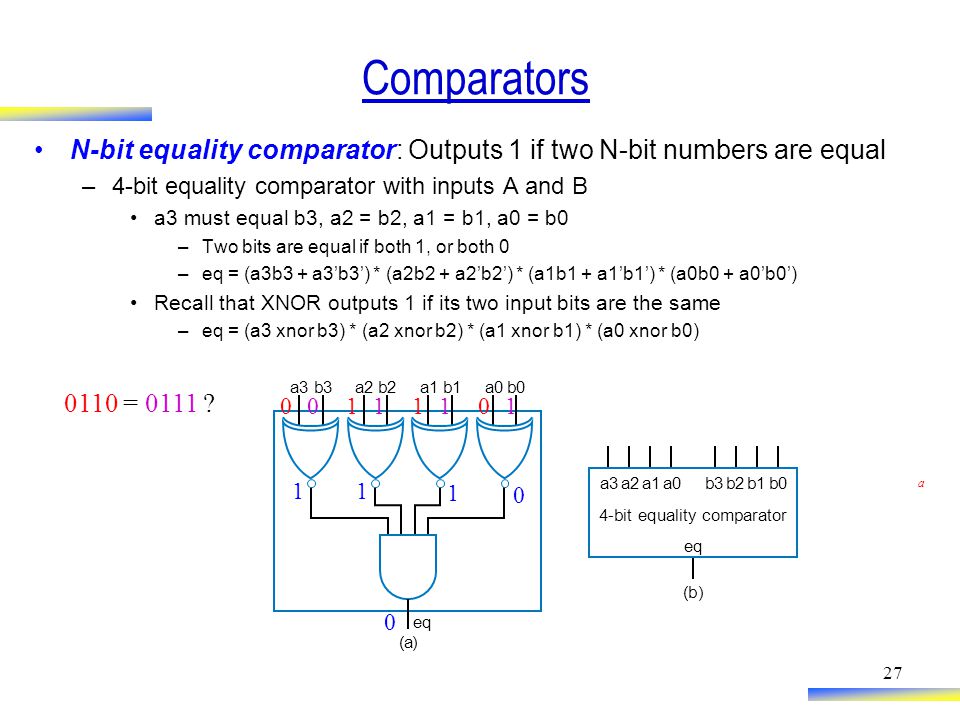
27 Comparators N-bit equality comparator: Outputs 1 if two N-bit numbers are equal –4-bit equality comparator with inputs A and B a3 must equal b3, a2 = b2, a1 = b1, a0 = b0 –Two bits are equal if both 1, or both 0 –eq = (a3b3 + a3’b3’) * (a2b2 + a2’b2’) * (a1b1 + a1’b1’) * (a0b0 + a0’b0’) Recall that XNOR outputs 1 if its two input bits are the same –eq = (a3 xnor b3) * (a2 xnor b2) * (a1 xnor b1) * (a0 xnor b0) a3b3a2b2a1b1a0b0 eq (a) (b) a3a2a1a0b3 eq b2b1b0 4-bit equality comparator a 0110 = 0111 ? 01100111 0 11 1 0
28
28 Magnitude Comparator N-bit magnitude comparator: Indicates whether A>B, A=B, or A<B, for its two N-bit inputs A and B –How design? Consider how compare by hand. First compare a3 and b3. If equal, compare a2 and b2. And so on. Stop if comparison not equal -- whichever’s bit is 1 is greater. If never see unequal bit pair, A=B. A=1011B=1001 10111001 a Equal 10111001Equal 10111001Unequal So A > B

29
29 Magnitude Comparator By-hand example leads to idea for design –Start at left, compare each bit pair, pass results to the right –Each bit pair called a stage –Each stage has 3 inputs indicating results of higher stage, passes results to lower stage Igt Ieq Ilt a3a2 a1a0 b3b2 b1b0 AgtB AeqB AltB in_gt in_eq in_lt out_gt out_eq out_lt Igt Ieq Ilt Stage 3 a3b3 ab in_gt in_eq in_lt out_gt out_eq out_lt Stage 2 a2b2 ab in_gt in_eq in_lt out_gt out_eq out_lt Stage 1 a1b1 ab in_gt in_eq in_lt out_gt out_eq out_lt AgtB AeqB AltB Stage 0 a0b0 ab (a) (b) 0 0 1 4-bit magnitude comparator
 (b) bit magnitude comparator")
30
30 Magnitude Comparator Each stage: –out_gt = in_gt + (in_eq * a * b’) A>B (so far) if already determined in higher stage, or if higher stages equal but in this stage a=1 and b=0 –out_lt = in_lt + (in_eq * a’ * b) A<B (so far) if already determined in higher stage, or if higher stages equal but in this stage a=0 and b=1 –out_eq = in_eq * (a XNOR b) A=B (so far) if already determined in higher stage and in this stage a=b too –Simple circuit inside each stage, just a few gates (not shown) in_gt in_eq in_lt out_gt out_eq out_lt Igt Ieq Ilt Stage 3 a3b3 ab in_gt in_eq in_lt out_gt out_eq out_lt Stage 2 a2b2 ab in_gt in_eq in_lt out_gt out_eq out_lt Stage 1 a1b1 ab in_gt in_eq in_lt out_gt out_eq out_lt AgtB AeqB AltB Stage 0 a0b0 ab
 A>B (so far) if already determined in higher stage, or if higher stages equal but in this stage a=1 and b=0 –out_lt = in_lt + (in_eq * a’ * b) A<B (so far) if already determined in higher stage, or if higher stages equal but in this stage a=0 and b=1 –out_eq = in_eq * (a XNOR b) A=B (so far) if already determined in higher stage and in this stage a=b too –Simple circuit inside each stage, just a few gates (not shown) in_gt in_eq in_lt out_gt out_eq out_lt Igt Ieq Ilt Stage 3 a3b3 ab in_gt in_eq in_lt out_gt out_eq out_lt Stage 2 a2b2 ab in_gt in_eq in_lt out_gt out_eq out_lt Stage 1 a1b1 ab in_gt in_eq in_lt out_gt out_eq out_lt AgtB AeqB AltB Stage 0 a0b0 ab")
31
31 Magnitude Comparator How does it work? in_gt in_eq in_lt out_gt out_eq out_lt Igt Ieq Ilt Stage3 a3b3 ab in_gt in_eq in_lt out_gt out_eq out_lt Stage2 a2b2 ab in_gt in_eq in_lt out_gt out_eq out_lt Stage1 a1b1 ab in_gt in_eq in_lt out_gt out_eq out_lt AgtB AeqB AltB Stage0 a0b0 11001011 ab (a) = 0 1 0 in_gt in_eq in_lt out_gt out_eq out_lt Igt Ieq Ilt Stage3 a3b3 ab in_gt in_eq in_lt out_gt out_eq out_lt Stage2 a2b2 ab in_gt in_eq in_lt out_gt out_eq out_lt Stage1 a1b1 ab in_gt in_eq in_lt out_gt out_eq out_lt AgtB AeqB AltB Stage0 a0b0 11001011 ab (b) 0 1 0 = 0 1 0 1011 = 1001 ? 0 1 0 Ieq=1 causes this stage to compare a
 = in_gt in_eq in_lt out_gt out_eq out_lt Igt Ieq Ilt Stage3 a3b3 ab in_gt in_eq in_lt out_gt out_eq out_lt Stage2 a2b2 ab in_gt in_eq in_lt out_gt out_eq out_lt Stage1 a1b1 ab in_gt in_eq in_lt out_gt out_eq out_lt AgtB AeqB AltB Stage0 a0b ab (b) = = Ieq=1 causes this stage to compare a.")
32
32 Magnitude Comparator Final answer appears on the right Takes time for answer to “ripple” from left to right Thus called “carry-ripple style” after the carry-ripple adder –Even though there’s no “carry” involved 1011 = 1001 ? in_gt in_eq in_lt out_gt out_eq out_lt Igt Ieq Ilt Stage3 a3b3 ab in_gt in_eq in_lt out_gt out_eq out_lt Stage2 a2b2 ab in_gt in_eq in_lt out_gt out_eq out_lt Stage1 a1b1 ab in_gt in_eq in_lt out_gt out_eq out_lt AgtB AeqB AltB Stage0 a0b0 11001011 ab (c) 0 1 0 1 0 0 > in_gt in_eq in_lt out_gt out_eq out_lt Igt Ieq Ilt Stage3 a3b3 ab in_gt in_eq in_lt out_gt out_eq out_lt Stage2 a2b2 ab in_gt in_eq in_lt out_gt out_eq out_lt Stage1 a1b1 ab in_gt in_eq in_lt out_gt out_eq out_lt AgtB AeqB AltB Stage0 a0b0 11001011 ab (d) 0 1 0 0 1 0 a
 > in_gt in_eq in_lt out_gt out_eq out_lt Igt Ieq Ilt Stage3 a3b3 ab in_gt in_eq in_lt out_gt out_eq out_lt Stage2 a2b2 ab in_gt in_eq in_lt out_gt out_eq out_lt Stage1 a1b1 ab in_gt in_eq in_lt out_gt out_eq out_lt AgtB AeqB AltB Stage0 a0b ab (d) a.")
33
33 Magnitude Comparator Example: Minimum of Two Numbers Design a combinational component that computes the minimum of two 8-bit numbers –Solution: Use 8-bit magnitude comparator and 8-bit 2x1 mux If A<B, pass A through mux. Else, pass B. MIN Igt Ieq Ilt AgtB AeqB AltB 0 1 0 A AB B 8-bit magnitude comparator s I1I0 2x1 mux 8-bit C 8 8888 8 8 8 C AB Min (a) (b) 1100000001111111 0 0 1 a
 (b) a.")
Similar presentations
>")


 — conventions define relationship between bits and numbers Binary numbers (base 2) 0000 0001 0010 0011 0100.>")
