Download presentation
Presentation is loading. Please wait.

1
Implementing Logic Gates and Circuits Discussion D5.1

2
Implementing Logic Gates and Circuits Logic With Relays Integrated Circuit Implementation of Gates Transistor-Transistor Logic (TTL) Programmable Logic Devices (PLDs) Complex Programmable Logic Devices (CPLDs) Field Programmable Gate Arrays (FPGAs)
 Programmable Logic Devices (PLDs) Complex Programmable Logic Devices (CPLDs) Field Programmable Gate Arrays (FPGAs)")
3
Relays Normally Open Relay A B C A B C Normally Closed Relay A-B closed when C = 1 (current through coil) A-B open when C = 1 (current through coil)
 A-B open when C = 1 (current through coil)")
4
NOT Gate 5V X Y 0 1 closed open X Y 0101 1010

5
NOT Gate 5V X Y 0 1 closed open X Y 0101 1010

6
AND Gate X Y Z 0 0 0 0 1 0 1 0 0 1 1 1 X Y Z 5V X Y Z

7
AND Gate X Y Z 0 0 0 0 1 0 1 0 0 1 1 1 X Y Z 5V X Y Z 0 0

8
AND Gate X Y Z 0 0 0 0 1 0 1 0 0 1 1 1 X Y Z 0 1

9
AND Gate X Y Z 0 0 0 0 1 0 1 0 0 1 1 1 X Y Z 1 0

10
AND Gate X Y Z 0 0 0 0 1 0 1 0 0 1 1 1 X Y Z 1 1

11
OR Gate X Y Z 0 0 0 0 1 1 1 0 1 1 1 1 5V X Y Z X Y Z

12
OR Gate X Y Z 0 0 0 0 1 1 1 0 1 1 1 1 5V X Y Z X Y Z 0 0

13
OR Gate X Y Z 0 0 0 0 1 1 1 0 1 1 1 1 X Y Z 0 1

14
OR Gate X Y Z 0 0 0 0 1 1 1 0 1 1 1 1 X Y Z 1 0

15
OR Gate X Y Z 0 0 0 0 1 1 1 0 1 1 1 1 X Y Z 1 1

16
Implementing Gates Using MOSFET Integrated Circuits Relays Normally open Normally closed A B C A B C A B C nMOS transistor A-B closed when C = 1 (normally open) pMOS transistor A-B closed when C = 0 (normally closed)
 pMOS transistor A-B closed when C = 0 (normally closed)")
17
NOT Gate 5V XY Y = X' X Y X Y 0101 1010

18
NOT Gate 5V XY Y = X' X Y 0 1 X Y 0101 1010

19
NOT Gate 5V XY Y = X' X Y 1 0 X Y 0101 1010

20
NAND Gate X Y Z 5V X Y Z X Y Z 0 0 1 0 1 1 1 0 1 1 1 0

21
NAND Gate X Y Z 5V X Y Z X Y Z 0 0 1 0 1 1 1 0 1 1 1 0 0 0

22
NAND Gate X Y Z 5V X Y Z X Y Z 0 0 1 0 1 1 1 0 1 1 1 0 0 1

23
NAND Gate X Y Z 5V X Y Z X Y Z 0 0 1 0 1 1 1 0 1 1 1 0 1 0

24
NAND Gate X Y Z 5V X Y Z X Y Z 0 0 1 0 1 1 1 0 1 1 1 0 1 1

25
NOR Gate X Y Z 5V X Y Z X Y Z 0 0 1 0 1 0 1 0 0 1 1 0

26
NOR Gate X Y Z 5V X Y Z X Y Z 0 0 1 0 1 0 1 0 0 1 1 0 0 0

27
NOR Gate X Y Z 5V X Y Z X Y Z 0 0 1 0 1 0 1 0 0 1 1 0 0 1

28
NOR Gate X Y Z 5V X Y Z X Y Z 0 0 1 0 1 0 1 0 0 1 1 0 1 0

29
NOR Gate X Y Z 5V X Y Z X Y Z 0 0 1 0 1 0 1 0 0 1 1 0 1 1

30
AND Gate X Y 5V Z NAND-NOT

31
OR Gate X Y 5V Z NOR-NOT

32
Transmission Gate (TG)
")
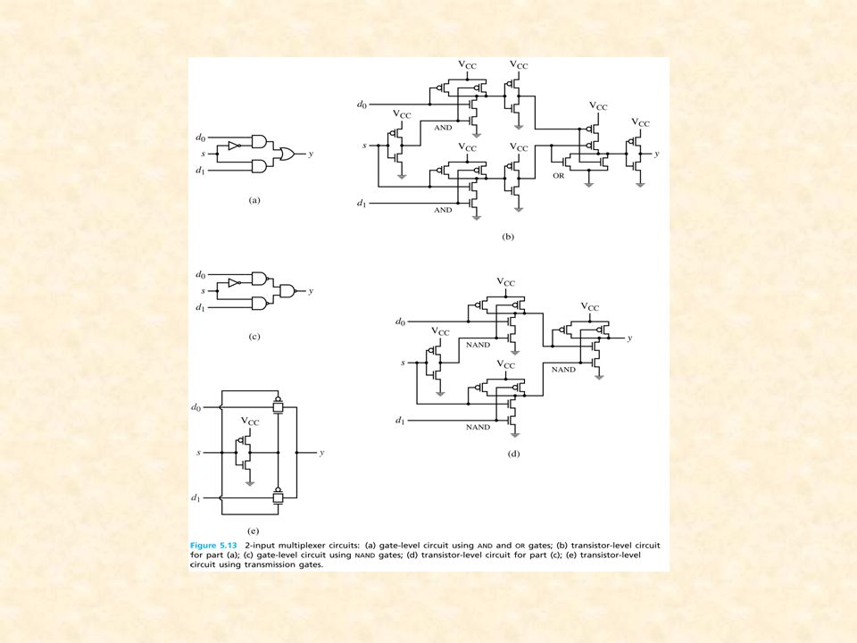
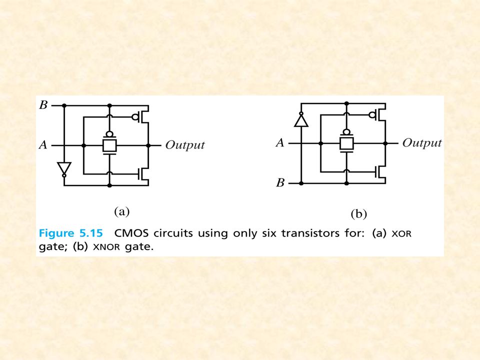
33
Selector and Exclusive- OR Constructed with Transmission Gates

39
Transistor-Transistor Logic (TTL) Developed in mid-1960s Large family (74xx) of chips from basic gates to arithmetic logic units Becoming obsolete with the development of programmable logic devices (PLDs)
 Developed in mid-1960s Large family (74xx) of chips from basic gates to arithmetic logic units Becoming obsolete with the development of programmable logic devices (PLDs)")
40
TTL Chips

41
TTL NAND, NOR, XOR

42
TTL Multiple-input Gates

43
Small-Scale Integrated (SSI) Circuits 1 to 10 gates NAND gate has 4 transistors
 Circuits 1 to 10 gates NAND gate has 4 transistors")
44
Medium-Scale Integrated (MSI) Circuits 10-100 gates Adders Comparators Multiplexers Decoders
 Circuits gates Adders Comparators Multiplexers Decoders")
45
Large-Scale Integrated (LSI) Circuits 100-1000 gates Arithmetic Logic Units
 Circuits gates Arithmetic Logic Units")
46
Very-Large-Scale Integrated (VLSI) Circuits >1000 gates Microprocessors Programmable Logic Devices (PLDs) Complex Programmable Logic Devices (CPLDs) Field Programmable Gate Arrays (FPGAs)
 Circuits >1000 gates Microprocessors Programmable Logic Devices (PLDs) Complex Programmable Logic Devices (CPLDs) Field Programmable Gate Arrays (FPGAs)")
47
Basic PLD Structure

48
Alternate PLD Representation

49
PLD Connections for XOR

50
1975 – Signetics invents the FPLA

51
1978 – MMI introduces the PAL

52
1983 – AMD introduces the 22V10 1984 – Lattice introduces the GAL – an electrically erasable PAL

53
The GAL 16V8 1 2 3 4 5 6 7 9 1011 12 8 19 20 17 18 15 16 13 14 GND Vcc I/CLK II/O I I I I I I I I/OE I/O GAL 16V8

54
Structure of the GAL 16V8 PLD

55
GAL 16V8 Input Buffer

56
Structure of the GAL 16V8 PLD

57
GAL 16V8 Polarity Control OE X A B C X closed B = 0 C = A open B = 1 C = A' Polarity Pin

58
Structure of the GAL 16V8 PLD

59
XC9500 CPLDs 5 volt in-system programmable (ISP) CPLDs 5 ns pin-to-pin 36 to 288 macrocells (6400 gates) Industry’s best pin- locking architecture 10,000 program/erase cycles Complete IEEE 1149.1 JTAG capability Function Block 1 JTAG Controller Function Block 2 I/O Function Block 4 3 Global Tri-States 2 or 4 Function Block 3 I/O In-System Programming Controller FastCONNECT Switch Matrix JTAG Port 3 I/O Global Set/Reset Global Clocks I/O Blocks 1
 CPLDs 5 ns pin-to-pin 36 to 288 macrocells (6400 gates) Industry’s best pin- locking architecture 10,000 program/erase cycles Complete IEEE JTAG capability Function Block 1 JTAG Controller Function Block 2 I/O Function Block 4 3 Global Tri-States 2 or 4 Function Block 3 I/O In-System Programming Controller FastCONNECT Switch Matrix JTAG Port 3 I/O Global Set/Reset Global Clocks I/O Blocks 1")
60
XC9500 Function Block To FastCONNECT From FastCONNECT 2 or 4 3 Global Tri-State Global Clocks I/O 36 Product- Term Allocator Macrocell 1 AND Array Macrocell 18 Each function block is like a 36V18 !

61
XC9500 Product Family 9536 Macrocells Usable Gates t PD (ns) Registers Max I/O 3672108144216 8001600240032004800 57.5 10 3672108144216 3472108133166 Packages VQ44 PC44 PC84 TQ100 PQ100 PC84 TQ100 PQ100 PQ160 PQ100 PQ160 288 6400 10 288 192 HQ208 BG352 PQ160 HQ208 BG352 957295108951449521695288
 Registers Max I/O Packages VQ44 PC44 PC84 TQ100 PQ100 PC84 TQ100 PQ100 PQ160 PQ100 PQ HQ208 BG352 PQ160 HQ208 BG")
62
Xilinx 95108 6 function blocks –Each contains 18 macro cells –Each macro cell behaves like a GAL32V18 AND-OR array for sum-of-products 32 inputs and 18 outputs

63
Architecture of the Xilinx XC95108 CPLD

64
PLDT-3 Xilinx XC95108 CPLD 7 segment display Switches LEDs Buttons

65
PLDT-3 12 macro cells connected to I/O pins 4 pushbuttons 8 toggle switches 8 dip switches 16 LEDs 2 7-segment displays On-board clock signals (4 MHz and 1 Hz)
")
66
FPGAs Field Programmable Gate Arrays

67
1985 – Xilinx introduces the LCA (Logic Cell Array) The Xilinx XC3000 CLB (configurable logic block).
 The Xilinx XC3000 CLB (configurable logic block).")
68
Programmable Interconnect I/O Blocks (IOBs) Configurable Logic Blocks (CLBs) 1991 – Xilinx introduces the XC4000 Architecture XC4003 contained 440,000 transistors 0.7-micron process
 Configurable Logic Blocks (CLBs) 1991 – Xilinx introduces the XC4000 Architecture XC4003 contained 440,000 transistors 0.7-micron process")
69
XC4000E/X Configurable Logic Blocks 2 Four-input function generators (Look Up Tables) - 16x1 RAM or Logic function 2 Registers - Each can be configured as Flip Flop or Latch - Independent clock polarity - Synchronous and asynchronous Set/Reset
 - 16x1 RAM or Logic function 2 Registers - Each can be configured as Flip Flop or Latch - Independent clock polarity - Synchronous and asynchronous Set/Reset")
70
Look Up Tables Capacity is limited by number of inputs, not complexity Choose to use each function generator as 4 input logic (LUT) or as high speed sync.dual port RAM Combinatorial Logic is stored in 16x1 SRAM Look Up Tables (LUTs) in a CLB Example: A B C D Z 0 0 0 0 0 0 0 0 1 0 0 0 1 0 0 0 0 1 1 1 0 1 0 0 1 0 1 0 1 1... 1 1 0 0 0 1 1 0 1 0 1 1 1 0 0 1 1 1 1 1 Look Up Table Combinatorial Logic A B C D Z 4-bit address G Func. Gen. G4 G3 G2 G1 WE 2 (2 ) 4 = 64K !
 4 = 64K !.")
71
What’s Really In that Chip? CLB (Red) Switch Matrix Long Lines (Purple) Direct Interconnect (Green) Routed Wires (Blue) Programmable Interconnect Points, PIPs (White)
 Switch Matrix Long Lines (Purple) Direct Interconnect (Green) Routed Wires (Blue) Programmable Interconnect Points, PIPs (White).")
72
1998 – Xilinx introduces the Virtex®™ FPGA family 0.25-micron process

73
2003 – Xilinx introduces the Spartan®™-3 family of products Very low cost World’s first 90 nm FPGA

74
Block diagram of Xilinx Spartan IIE FPGA

75
Each Spartan IIE CLB contains two of these CLB slices

76
Block diagram of Xilinx Spartan-3 FPGA

77
Each Spartan-3 CLB contains four CLB slices

78
Spartan 3 Board

79
CPLDs vs. FPGAs

80
x Xilinx will release the world’s first one-billion transistor device this year

Similar presentations


 –Up to 57 Kb block RAM storage Flexible.>")


 CPLDs 5 ns pin-to-pin 36 to 288 macrocells (6400 gates) Industry’s.>")

 Lecture L4.1. Transistor-Transistor Logic (TTL) Developed in mid-1960s Large family (74xx) of chips from basic gates.>")


 The slides included herein were taken.>")
 Programmable.>")