Download presentation
Presentation is loading. Please wait.

1
Ch6 DC-DC Converters 6-1 Linear voltage regulators Fig. 6.1 Adjustingbasecurrent, => linear DC-DC converter orlinear regulator Thetransistor operates in the linear region. Low efficiency happen under lower output voltage. => improved by switching converter.

2
6-2A basic switching converter. Fig. 6.2 The transistor operates as an electronic switch and in saturation state.

3
If the ideal switch is assumed, the energy efficiency is 100%

4
6-3 The Buck converter (Down converter) Fig.6.3, Fig.6.4 → To produce an output that is purely dc. Properties:

6
Assumptions: (1) In steady state (2) is constant ( positive ) (3) is constant ( C is very large) (4) Closed time=DT, open time=(1-D)T (5) Components are ideal Sw. closed : increases linearly

7
Sw. open : decrease linearly Steady-state operation requires that the inductor current at the end of the switching cycle is the same as that at the beginning, meaning that the net change in inductor current over one period is zero.

8
= 0 Since the average inductor voltage is zero for periodic operation

9
Average Current Imax= Imin= Since Imin = 0 is the boundary between continuous and discontinuous Imin = 0 =

11
In practice, the output voltage cannot be kept perfectly constant with a finite capacitance. Fig. 6.5

13
6-4 Design considerations Buck Converter: ↑, Lmin↓,Cmin↓, P loss in switches↑, heat sink ↑ The inductor wire must be rated at the rms current, and the core should not saturate for peak inductor current.The capacitor must be selected to limit the output ripple to the design specifications, to withstand peak output voltage, and to carry the required rms current. The switch and diode must withstand maximum voltage stress when off and maximum current when on. The temperature ratings must not be exceeded, possibly requiring a heat sink.

14
6-5 The boost converterFig 6-6 The output voltage is larger than the input

15
Assumptions: (1) In steady-state. (2) The switch is closed for time DT and open for (1-D)T. (3) The inductor current is continuous (positive). (4) The capacitor is very large, and is held constant. (5) Components are ideal. Fig 6-7 When the switch is closed: increases linearly
 The inductor current is continuous (positive). (4) The capacitor is very large, and is held constant. (5) Components are ideal. Fig 6-7 When the switch is closed: increases linearly.")
17
When the switch is open: must change linearly For steady-state, the net change in inductor current must be zero.

18
The average inductor voltage must be zero for periodic operation Output power: Input power -----------Inductor Current

19
Imax = Imin = The boundary between continuous and discontinuous inductor current is determined form.

20
The change in capacitor charge f: switching frequency.

21
6-6 The Buck-Boost converter Fig 6-8 The out voltage can be either higher or lower than the input, and there is a polarity reversal on the output.

22
Assumptions: (1) In steady-state. (2) is continuous. (3) is held constant. (4) The switch is closed for time DT and open for (1-D)T. (5) Components are ideal. When the switch is closed. increases linearly.
 is held constant. (4) The switch is closed for time DT and open for (1-D)T. (5) Components are ideal. When the switch is closed. increases linearly..")
23
When the switch is open: The average inductor voltage is zero for periodic operation. can be less than the source or greater than the source.

25
Imax = Imin = For continuous : Imin = 0 : switching fre.

27
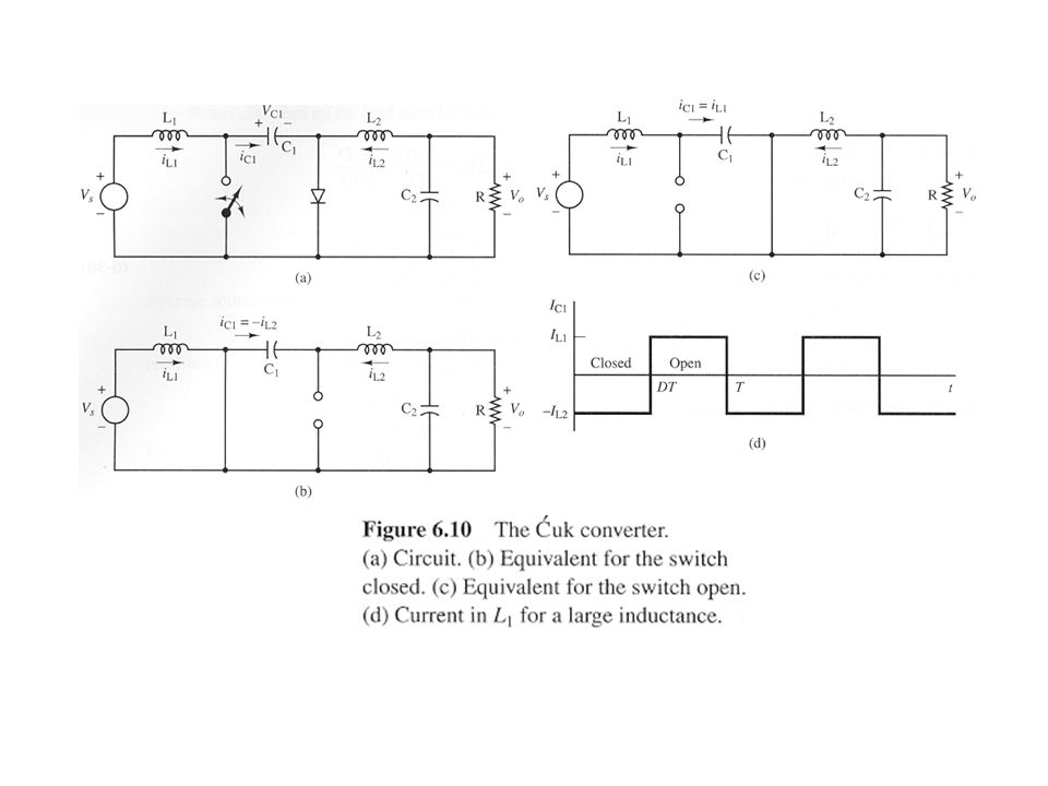
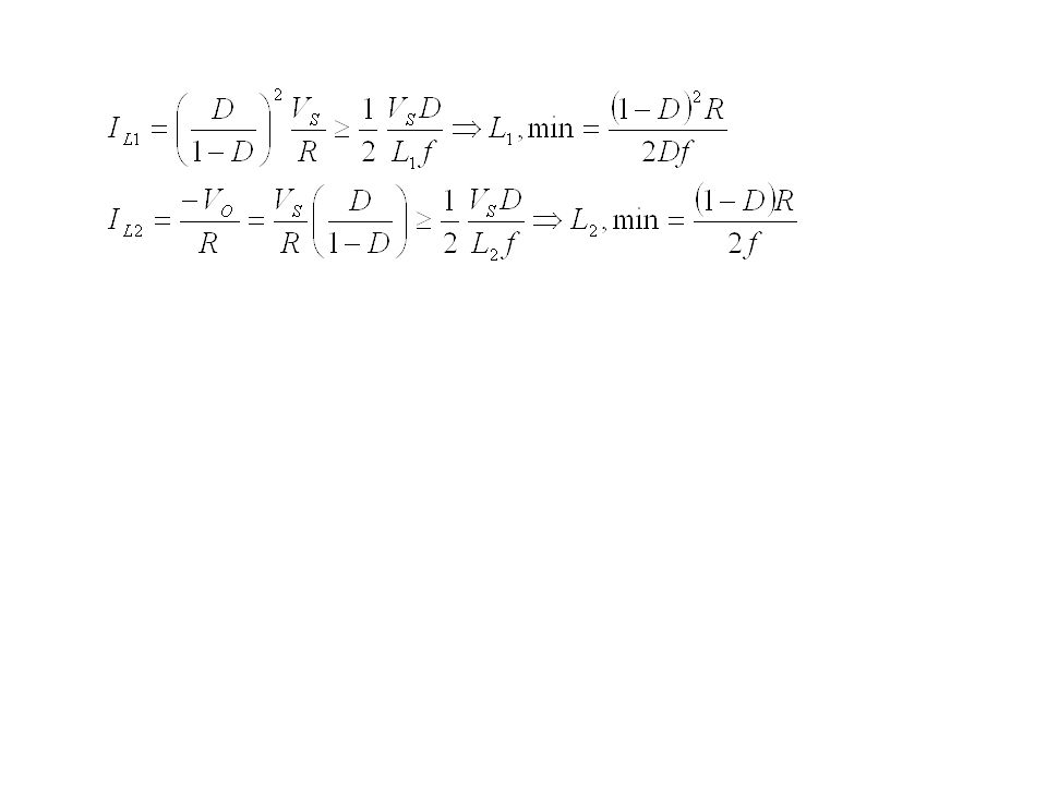
6-7 The ‘Cuk converter Fig 6-10 Output voltage magnitude can be either larger or smaller than the input, and there is a polarity reversal on the output. Assumptions: (1) are very large and the currents in them are constant. (2) are very large and the voltage across them are constant. (3) In steady-state. (4) The switch is closed for time DT and open for (1-D)T. (5) Switch and diode are ideal.
 are very large and the currents in them are constant. (2) are very large and the voltage across them are constant. (3) In steady-state. (4) The switch is closed for time DT and open for (1-D)T. (5) Switch and diode are ideal..")
29
Average voltage across i s With the switch closed, With the switch open, Average capacitor current is zero for periodic operation.

30
Since the components on the output ( ) are in the same configuration as the Buck converter, the output voltage ripple. The ripple in (Sw. is open, )
.")
31
When Sw. is closed, For continuous current in the inductors, the average current must be greater than one-half the change in current.

33
6-8 Non-ideal effects on converter performance Switch voltage drops: For Buck converter: With the switch closed,, : voltage drops across conducting switches. With the switch open,, : voltage drop across the diode. Average voltage across the inductor is zero for the switching period: is lower than for the ideal case.

34
Capacitor resistance : effect on ripple (For Buck converter) Real capacitor : ESR : equivalent series resistance.. ESL : equivalent series inductance ESR may produce a ripple greater than that of the capacitance. ESL is not a factor at low switching fre, but may be significant above perhaps 300KHZ. is obtained under the ideal capacitor. (6-15)
.")
35
Inductor resistance ( ): For Boost converter. Fig 6-11
: For Boost converter. Fig 6-11")
37
Efficiency of Boost converter: Switching losses : In addition to the on-state voltage drops and associated power losses of switches, additional losses occur in the switches as they turn on and off, seeing ( Fig6-12 (a) ), there are two types of different switch on-off transitions, ( Fig 6-12 (b) ) (power losses) may be closer to actual switching situations. Higher switching fre.→higher switching losses. Reducing switching losses: making switching occur at zero voltage and/or zero current. (Resonant converter)
.")
39
6-9 Discontinuous-current operation A different analysis is required for the discontinuous current ( ) case. Buck converter( Fig 6-13 ) Average inductor voltage is zero for periodic operation.
 Average inductor voltage is zero for periodic operation..")
41
When switch is closed Discontinuous current occurs when, and Imin will be zero.

42
Boost converter: Fig 6-15 Average voltage across the inductor:

43
Average diode current: Fig. 6.16 Discontinuous current ( ) occurs when, and Imin will be zero.
 occurs when, and Imin will be zero.")
Similar presentations


>")


 國立雲林科技大學 電子工程系>")


