Download presentation
Presentation is loading. Please wait.

1
EE462L, Fall 2011 DC−DC Buck/Boost Converter

2
Boost converter Buck/Boost converter
+ v L1 – i I in out L1 C + V V in out – Buck/Boost converter V in i L1 + v L1 – + v L2 – C1 + v C1 – L2 + V out – I C + v L2 – C1 + v C1 – L2

3
Buck/Boost converter V in i L1 + v L1 – + v L2 – C1 + v C1 – L2 + V out – I C This circuit is more unforgiving than the boost converter, because the MOSFET and diode voltages and currents are higher Before applying power, make sure that your D is at the minimum, and that a load is solidly connected Limit your output voltage to 90V

4
KVL and KCL in the average sense
+ Vin – + 0 – I I I in out out L1 + – + C1 I V out V in out I C L2 in – KVL shows that VC1 = Vin Interestingly, no average current passes from the source side, through C1, to the load side, and yet this is a “DC - DC” converter

5
Switch closed i I + L1 C1 V V C L2 – i I + L1 C1 V V C I L2 –
assume constant + Vin – + Vin – + v D – i + V out – I C in L1 + v L2 – C1 V in L2 KVL shows that vD = −(Vin + Vout), so the diode is open Thus, C is providing the load power when the switch is closed + Vin – – (Vin + Vout) + + Vin – i I in out L1 – Vin + + C1 V V in out C L2 I out – iL1 and iL2 are ramping up (charging). C1 is charging L2. C is discharging.
, so the diode is open. Thus, C is providing the load power when the switch is closed. + Vin – – (Vin + Vout) + + Vin – i. I. in. out. L1. – Vin. + + C1. V. V. in. out. C. L2. I. out. – iL1 and iL2 are ramping up (charging). C1 is charging L2. C is discharging.")
6
Switch open (assume the diode is conducting because, otherwise, the circuit cannot work)
assume constant + Vin – – Vout + i I in out L1 + + C1 V V V in out out C L2 – – C1 and C are charging. L1 and L2 are discharging. KVL shows that VL1 = −Vout The input/output equation comes from recognizing that the average voltage across L1 is zero

7
Inductor L1 current rating
During the “on” state, L1 operates under the same conditions as the boost converter L, so the results are the same Use max

8
Inductor L2 current rating
Average values + Vin – + 0 – I I I in out out L1 + – + C1 I V out V in out I C in L2 – iL2 2Iout Iavg = Iout ΔI Use max

9
MOSFET and diode currents and current ratings
+ v L2 – C1 + v C1 – L2 + v L1 – i I in out L1 + V V in out C – iL1 + iL2 MOSFET Diode iL1 + iL2 2(Iin + Iout) 2(Iin + Iout) switch closed switch open Take worst case D for each Use max
 2(Iin + Iout) switch. closed. switch. open. Take worst case D for each. Use max.")
10
Output capacitor C current and current rating
iC = (iD – Iout) 2Iin + Iout −Iout switch closed switch open As D → 1, Iin >> Iout , so As D → 0, Iin << Iout , so
 2Iin + Iout. −Iout. switch closed. switch open. As D → 1, Iin >> Iout , so. As D → 0, Iin << Iout , so.")
11
Series capacitor C1 current and current rating
+ Vin – – (Vin + Vout) + + Vin – i I in out L1 – Vin + + C1 V V in out C L2 I out – + Vin – – Vout + i I in out L1 + + C1 V V V in out out C L2 – – Switch closed, IC1 = −IL2 Switch open, IC1 = IL1
 + + Vin – i. I. in. out. L1. – Vin. + + C1. V. V. in. out. C. L2. I. out. – + Vin – – Vout + i. I. in. out. L C1. V. V. V. in. out. out. C. L2. – – Switch closed, IC1 = −IL2. Switch open, IC1 = IL1.")
12
Series capacitor C1 current and current rating
iC1 Switch closed, IC1 = −IL2 Switch open, IC1 = IL1 2Iin switch closed switch open −2Iout As D → 1, Iin >> Iout , so As D → 0, Iin << Iout , so

13
Worst-case load ripple voltage
iC = (iD – Iout) −Iout The worst case is where D → 1, where output capacitor C provides Iout for most of the period. Then,
 −Iout. The worst case is where D → 1, where output capacitor C provides Iout for most of the period. Then,")
14
Worst case ripple voltage on series capacitor C1
iC1 switch open 2Iin −2Iout switch closed Then, considering the worst case (i.e., D = 1)
")
15
Voltage ratings + L1 C1 V V C L2 – + L1 C1 V V C L2 – + Vin –
– (Vin + Vout) + L1 + C1 V V in out C L2 – MOSFET and diode see (Vin + Vout) + Vin – – Vout + L1 + C1 V V in out C L2 – Diode and MOSFET, use 2(Vin + Vout) Capacitor C1, use 1.5Vin Capacitor C, use 1.5Vout
 + L1. + C1. V. V. in. out. C. L2. – MOSFET and diode see (Vin + Vout) + Vin – – Vout + L1. + C1. V. V. in. out. C. L2. – Diode and MOSFET, use 2(Vin + Vout) Capacitor C1, use 1.5Vin. Capacitor C, use 1.5Vout.")
16
Continuous current in L1
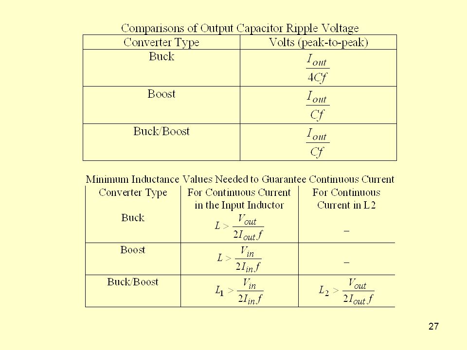
iL 2Iin Iavg = Iin (1 − D)T Then, considering the worst case (i.e., D → 1), use max guarantees continuous conduction use min
T. Then, considering the worst case (i.e., D → 1), use max. guarantees continuous conduction. use min.")
17
Continuous current in L2
iL 2Iout Iavg = Iout (1 − D)T Then, considering the worst case (i.e., D → 0), use max guarantees continuous conduction use min
T. Then, considering the worst case (i.e., D → 0), use max. guarantees continuous conduction. use min.")
18
Impedance matching Iin DC−DC Boost Converter + + Vin − − Source Iin +
Equivalent from source perspective

19
Impedance matching For any Rload, as D → 0, then Requiv → ∞ (i.e., an open circuit) For any Rload, as D → 1, then Requiv → 0 (i.e., a short circuit) Thus, the buck/boost converter can sweep the entire I-V curve of a solar panel

20
Example - connect a 100Ω load resistor
2Ω equiv. 6.44Ω equiv. D = 0.50 100Ω equiv. With a 100Ω load resistor attached, raising D from 0 to 1 moves the solar panel load from the open circuit condition to the short circuit condition

21
Example - connect a 5Ω load resistor
2Ω equiv. 6.44Ω equiv. D = 0.18 100Ω equiv.

22
Likely worst-case buck/boost situation
BUCK/BOOST DESIGN 5.66A p-p 200V, 250V 16A, 20A Our components 9A 250V 10A, 5A 10A 90V 40V, 90V Likely worst-case buck/boost situation 10A, 5A MOSFET M. 250V, 20A L1. 100µH, 9A C. 1500µF, 250V, 5.66A p-p Diode D. 200V, 16A L2. 100µH, 9A C1. 33µF, 50V, 14A p-p

23
BUCK/BOOST DESIGN 5A 0.067V 1500µF 50kHz L1. 100µH, 9A L2. 100µH, 9A
C. 1500µF, 250V, 5.66A p-p C1. 33µF, 50V, 14A p-p Diode D. 200V, 16A MOSFET M. 250V, 20A

24
BUCK/BOOST DESIGN 40V 90V 200µH 450µH 2A 50kHz 2A 50kHz L1. 100µH, 9A
C. 1500µF, 250V, 5.66A p-p C1. 33µF, 50V, 14A p-p Diode D. 200V, 16A MOSFET M. 250V, 20A

25
Likely worst-case buck/boost situation
BUCK/BOOST DESIGN Our components 9A 14A p-p 50V 10A A 40V Likely worst-case buck/boost situation 5A 33µF 50kHz 3.0V L1. 100µH, 9A L2. 100µH, 9A C. 1500µF, 250V, 5.66A p-p C1. 33µF, 50V, 14A p-p Diode D. 200V, 16A Conclusion - 50kHz may be too low for buck/boost converter MOSFET M. 250V, 20A

Similar presentations


>")


 國立雲林科技大學 電子工程系>")


