Download presentation
Presentation is loading. Please wait.

1
Design and Layout Guidelines
Robert Benjamin Applications Engineer

2
Information Sources

3
Information Sources King Solomon: Book of Proverbs 15:22
Plans go wrong for lack of advice; many advisers bring success. 15:31 If you listen to constructive criticism you will be at home among the wise.

4
Information Sources Internet/Magazines (Printed Circuit Design and Fabrication) Trade Organizations (IPC, JEDEC, IEEE, SMTA) TI Internal Sites Your Neighbor

5
Interference

6
Interference RFI EMI ESD Crosstalk and Feedback Phones (Cell and Home)
Broadcast Stations Wireless Technologies (Computers, Blu-Tooth, Tablets) EMI Motors Electrical Equipment Power Sources (Man Made and Natural) ESD Crosstalk and Feedback Interference can come from a variety of sources. Some of this can come from desired sources, like RF used for communications, that undesirably get into the circuit. Others are generated sources, like EMI from motors and electrical equipment that operates around us that generate and electro-magnetic fields. EMI can also appear for power generating and transmission sources. It can also appear in natural phenomena like lightning. ESD is also a very common problem as static sources are very common, and the human body can also carry a charge so that if we come in contact with devices or equipment contact can cause damage or interruption of operation. Crosstalk and feedback can play interference roles as well. Crosstalk is one signal coupling into a near by signal. Feedback is simply an output signal that affects the input. This can be either positive or negative and can affect results. The interference can be dealt with a number of ways. Sometimes with shielding, and often with some form of filtering. The effectiveness of the filter will depend on design and layout.
 EMI. Motors. Electrical Equipment. Power Sources (Man Made and Natural) ESD. Crosstalk and Feedback. Interference can come from a variety of sources. Some of this can come from desired sources, like RF used for communications, that undesirably get into the circuit. Others are generated sources, like EMI from motors and electrical equipment that operates around us that generate and electro-magnetic fields. EMI can also appear for power generating and transmission sources. It can also appear in natural phenomena like lightning. ESD is also a very common problem as static sources are very common, and the human body can also carry a charge so that if we come in contact with devices or equipment contact can cause damage or interruption of operation. Crosstalk and feedback can play interference roles as well. Crosstalk is one signal coupling into a near by signal. Feedback is simply an output signal that affects the input. This can be either positive or negative and can affect results. The interference can be dealt with a number of ways. Sometimes with shielding, and often with some form of filtering. The effectiveness of the filter will depend on design and layout.")
7
Circuit Issues

8
Key Circuit Issues Drift Linearity EMI/RFI Protection
Component Selection

9
DC drift Every component is a potential drift source;
but the reference usually out-drifts them all! The errors of the reference can be removed by using the excitation voltage for the reference voltage. Care must be observed when setting up a ratiometric system that the excitation voltage and the reference voltage are actually the same voltage. Extra resistance or inductance in one of the paths could lead to a mismatch in the two voltages which would lead to a loss in the benefits that normally derive from ratiometric measurements. Other required capacitors in the signal path could lead to a drift in the measurement. The amount of drift is directly related to the qualities of the capacitors. Parasitic thermocouples can also cause drift – watch out!

10
In-circuit Thermocouples
All connections between two different metals will create a thermocouple. This will occur many times as the signal travels from the sensor to the amplifier or Analog to Digital converter. All measurement systems have these same thermocouples, but they are only a problem if there is a temperature differential between the two thermocouples of the same metals. If the thermocouples can be kept close together or protected with solid metal bars so that they stay at the same temperature, then these thermocouples will not affect the measurement. But if there are thermal gradients across the board that cause these junctions to be at different temperatures, then you will have an added voltage that will drift with the changes in these temperatures.

11
DC linearity Keep reference impedance low C0G caps if possible
C0G capacitors are a definite improvement over some of the lower cost capacitor dielectrics such as X7R and Z5U. However, even C0G has some drift. Good results have been achieved using polyphenylene sulfide (PPS) dielectrics in these applications. This is particularly critical for those capacitors in the signal path. Consider driving differentially – also improves dynamic range Keep front-end balanced
 dielectrics in these applications. This is particularly critical for those capacitors in the signal path. Consider driving differentially – also improves dynamic range. Keep front-end balanced.")
12
EMI/RFI Protection Inductors – Ferrites, Coils
Capacitive Filters – Feed-Thru, X2Y Warning: Adding inductance to/through the ground connections will create more problems than it solves. Do NOT bridge Analog and Digital grounds with an inductor. A number of methods can be used for EMI/RFI filtering and protection. Ferrite cable clamps can be added to power and sensor cabling. For AC power filtering, the common-mode coil or transformer has two windings separated with sufficient spacing between coils windings to prevent high voltage breakdown. The windings follow the dot convention such that their magnetic fields are in phase internal to the core. The differential filter can be made to have greater attenuation by reducing the filter’s cut-off frequency. The leakage inductance on it’s own is sufficient to be used for a lower frequency filter, but a differential-mode inductor can be added in series with each input to the common-mode coils to lower the cutoff frequency. Although the inductors shown are suitable for AC line filters, properly specified common-mode and differential-mode inductors may be utilized in EMI filter from DC to RF. R-C filters are an inexpensive method of filtering all types of signals, especially in the analog signal path. Care must be taken to only use a high grade of capacitor in this path. C0G and X2Y caps are acceptable, as are film and other PPS caps. X2Y, or the similar feed-thru type caps, can be a very affective means of filtering unwanted signals from the digital lines.

13
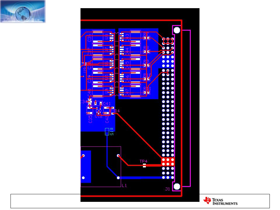
External ESD Protection
A Need May Arise for Extra ESD Protection Schottky Diodes. Transient Voltage Suppression (TVS). ESD Protection Device ICs (TPD4E001.) Schottky or TVS diodes can be used as added external protection for ESD events. Transient protection devices, like the TPD4E001 (and it’s sister parts,) can add protection in an easy to connect package. One thing to consider for both ESD and EMI/RFI is the grounding on the board. Ground loops, that can pick up external events, can be detrimental to your system even with a good design. So layout is critical to performance, and that will be discussed later.
. ESD Protection Device ICs (TPD4E001.) Schottky or TVS diodes can be used as added external protection for ESD events. Transient protection devices, like the TPD4E001 (and it’s sister parts,) can add protection in an easy to connect package. One thing to consider for both ESD and EMI/RFI is the grounding on the board. Ground loops, that can pick up external events, can be detrimental to your system even with a good design. So layout is critical to performance, and that will be discussed later.")
14
Moving from Circuit to Layout

15
Different Tasks Require Different Caps
Capacitor Selection Different Tasks Require Different Caps Bulk (Tantalum, MLCC) Bypass/Filter (MLCC-C0G, X2Y, X7R) Signal Path (Mica, PPS, Film, MLCC-C0G) Not all capacitors a equal in terms of size and performance. If a large bulk capacitance is needed as a charge reservoir, then some types of capacitor are out of the question. They would just be too physically large and cost prohibitive. In some cases a little ESR is ok to prevent oscillation from op amp circuits. In this case a tantalum or lower grade MLCC (multi-layer ceramic chip) capacitor may be just fine for the application. These bulk capacitors may range from 10uF and up to well over 200uF. The higher capacitance values are probably better served with tantalum. For bypassing and filtering MLCC is most often used for values under 100uF. X2Y and C0G are the better grades to use. C0G is usually limited to 10nF maximum capacitance. For the analog signal path, C0G capacitors are a definite improvement over some of the lower cost capacitor dielectrics such as X7R and Z5U. However, even C0G has some drift. Good results have been achieved using polyphenylene sulfide (PPS) dielectrics in these applications. Silver mica has very good characteristics, and outperforms C0G. PPS and silver mica perform similarly, but they are both physically larger than the C0G caps. X2Y caps have very good results, and can replace the need for common mode caps when used as a differential cap. This will be discussed later.
 Bypass/Filter (MLCC-C0G, X2Y, X7R) Signal Path (Mica, PPS, Film, MLCC-C0G) Not all capacitors a equal in terms of size and performance. If a large bulk capacitance is needed as a charge reservoir, then some types of capacitor are out of the question. They would just be too physically large and cost prohibitive. In some cases a little ESR is ok to prevent oscillation from op amp circuits. In this case a tantalum or lower grade MLCC (multi-layer ceramic chip) capacitor may be just fine for the application. These bulk capacitors may range from 10uF and up to well over 200uF. The higher capacitance values are probably better served with tantalum. For bypassing and filtering MLCC is most often used for values under 100uF. X2Y and C0G are the better grades to use. C0G is usually limited to 10nF maximum capacitance. For the analog signal path, C0G capacitors are a definite improvement over some of the lower cost capacitor dielectrics such as X7R and Z5U. However, even C0G has some drift. Good results have been achieved using polyphenylene sulfide (PPS) dielectrics in these applications. Silver mica has very good characteristics, and outperforms C0G. PPS and silver mica perform similarly, but they are both physically larger than the C0G caps. X2Y caps have very good results, and can replace the need for common mode caps when used as a differential cap. This will be discussed later.")
16
Signal Paths Require Quality Caps THD+N vs
Signal Paths Require Quality Caps THD+N vs. Voltage for Various Capacitor Types Capacitors have a voltage coefficient, which means that the capacitance changes with applied voltage. This also tends to be nonlinear, and thus introduces distortion which changes with frequency. Here is a look at several capacitor types and their distortion versus voltage characteristics. The second lowest line on this chart is the system measurement limit - and the line right next to that is a silver-mica capacitor (which is lower because the cap is limiting the bandwidth and thus reduces the noise measured). The other lines on this chart are from ceramic caps with different dielectrics - Z5U, Y5V, and X7R. Note that these types introduce significant distortion into the signal. One ceramic dielectric, the C0G type, closely matches the silver mica performance (but is not shown on this chart). The polyphenylene sulfide capacitors will also match the performance of silver mica.
. The other lines on this chart are from ceramic caps with different dielectrics - Z5U, Y5V, and X7R. Note that these types introduce significant distortion into the signal. One ceramic dielectric, the C0G type, closely matches the silver mica performance (but is not shown on this chart). The polyphenylene sulfide capacitors will also match the performance of silver mica.")
17
The X2Y Advantage Shorter current path, Smaller current loops
Dual parallel current paths to ground reduce inductance Opposing current flow reduces mutual inductance by cancellation. The structure is balanced, resulting in exceptional common mode filtering. X2Y is typically 1/10th the inductance of a like-sized conventional MLCC. Unlike MLCCs, inductance does not increase with size. There are a number of advantages for using a X2Y cap versus a regular MLCC cap. The construction of the X2Y cap allows for electrodes to be placed on the sides of the cap. This radically reduces the inductance of the cap as there is a much shorter current path from end to end, and the current loops become much smaller. There are also dual current paths to ground, which will reduce the overall inductance of the device. This feature is a benefit as the inductance does not increase with increasing size of the device. Also, the typical inductance is very small as compared to a comparable sized MLCC of another type. Due to the low inductance and balanced nature of the capacitor, the device provides exceptional common mode filtering. When the X2Y is used across a differential input, additional common mode caps are not needed. This provides excellent filtering with fewer components.

18
PCB Layout Tips

19
Basic PCB Design Principles
Separate Analog and Digital Signals Pay Close Attention on Connecting AGND and DGND Provide Good Ground Return Paths High Frequency Bypassing Minimize Inductance (Vital for HS) Control Thermocouples Fill void areas on signal layers with ground fill. Taking care of these things will also help improve EMI/RFI performance. The separation of the Analog and Digital section of the PCB keeps noisy digital from the low level analog. However, they must come together at the ADC or DAC. It is important that the Analog Ground and the Digital Ground be connected together at the ADC or DAC. This allows a quick return for the ground currents as the analog and digital portions of the device communicate. Inductance is determined by the size of the loop of current. Providing a path for return currents next to the signal trace will reduce the inductance. That is the advantage of a solid ground plane. If a reasonably solid plane can’t be achieved with two layers, then more layers should be used. Following these principles also helps to reduce the susceptibility of the circuit to RF interference (RFI) and reduce radiated noise (EMI).
 Control Thermocouples. Fill void areas on signal layers with ground fill. Taking care of these things will also help improve EMI/RFI performance. The separation of the Analog and Digital section of the PCB keeps noisy digital from the low level analog. However, they must come together at the ADC or DAC. It is important that the Analog Ground and the Digital Ground be connected together at the ADC or DAC. This allows a quick return for the ground currents as the analog and digital portions of the device communicate. Inductance is determined by the size of the loop of current. Providing a path for return currents next to the signal trace will reduce the inductance. That is the advantage of a solid ground plane. If a reasonably solid plane can’t be achieved with two layers, then more layers should be used. Following these principles also helps to reduce the susceptibility of the circuit to RF interference (RFI) and reduce radiated noise (EMI).")
20
Traces

21
Board Traces Traces Can Act Like Antennas
Traces Have Transmission Line Properties Inductance Resistance Traces for Power Should be Wide Connect and Terminate Effectively (vias) The separation of the Analog and Digital section of the PCB keeps noisy digital from the low level analog. However, they must come together at the ADC or DAC. It is important that the Analog Ground and the Digital Ground be connected together at the ADC or DAC. This allows a quick return for the ground currents as the analog and digital portions of the device communicate. Inductance is determined by the size of the loop of current. Providing a path for return currents next to the signal trace will reduce the inductance. That is the advantage of a solid ground plane. If a reasonably solid plane can’t be achieved with two layers, then more layers should be used. Following these principles also helps to reduce the susceptibility of the circuit to RF interference (RFI) and reduce radiated noise (EMI).
 The separation of the Analog and Digital section of the PCB keeps noisy digital from the low level analog. However, they must come together at the ADC or DAC. It is important that the Analog Ground and the Digital Ground be connected together at the ADC or DAC. This allows a quick return for the ground currents as the analog and digital portions of the device communicate. Inductance is determined by the size of the loop of current. Providing a path for return currents next to the signal trace will reduce the inductance. That is the advantage of a solid ground plane. If a reasonably solid plane can’t be achieved with two layers, then more layers should be used. Following these principles also helps to reduce the susceptibility of the circuit to RF interference (RFI) and reduce radiated noise (EMI).")
22
Return Currents Analog Digital Source Signal Return Current
Care must be observed to be sure that the signals have a good return current path. The current will follow the path of least impedance. The inductance of a path is determined by the loop area that it encloses. The larger the area the current has to travel to return to the source, the larger the inductance. The smallest inductance path is directly next to the trace. If the trace is over a solid ground plane, then the return current will travel in that ground plane directly below the signal trace. If the ground plane is cut or has other traces that block the current from flowing right next to the signal trace, it will have to find another path to return to the source and complete the circuit. If it is forced into a larger path, that will increase the chances that the signal will radiate and that sensitive signals will be more susceptible to EMI interference. Source Signal Return Current

23
Loop Inductance The area enclosed by the source signal and it’s return current will determine the inductance in the path. The larger the area, the higher the inductance. These diagrams show how the current flows when trying to find the path of least inductance. The return current will attempt to flow in the ground lead right next to the source signal if it can. However, if the ground return path is interrupted, then it will have to find a longer route (higher inductance) until it can return to a path that closely follows the source. Source: Analog and Mixed-Signal Products August 2000 Analog Applications Journal
 until it can return to a path that closely follows the source. Source: Analog and Mixed-Signal Products August 2000 Analog Applications Journal.")
24
PCB Layout Tips High Resolution Measurements
1 inch 1.3µV 10µA 1 inch (7 mil) trace of 1/2 oz copper with 10μA of current => voltage drop of 1.3μV 4 LSBs (298nV) at 24 bits! You must be careful with the PCB layout for a 12 bit design. For a 16-bit design you have to do everything correctly to achieve that performance; it should be obvious that a 24-bit design will be affected by any errors in the layout.
 trace of 1/2 oz copper with 10μA of current => voltage drop of 1.3μV. 4 LSBs (298nV) at 24 bits! You must be careful with the PCB layout for a 12 bit design. For a 16-bit design you have to do everything correctly to achieve that performance; it should be obvious that a 24-bit design will be affected by any errors in the layout.")
25
PCB Traces Resistive AND Inductive 1 inch 0.5 cm trace
Resistance = ohms Inductance = 20 nH Current change of 100 mA in 30 nS Resistive Voltage of 250 uV Inductive Voltage of 70 mV The inductance of a trace can be more serious and create a larger impedance than the resistance. We must take care to reduce the inductance. This can be done by minimizing loop area and keeping traces as short as possible. Note that vias in a board have twice the inductance of an equivalent length wire. Keeping the ground plane continuous reduces loop areas and inductance.

26
PCB Traces and Caps Example – Reference Circuit (REF50xx or Buffered by OPA350) Schematic Layout 1/(2p (L * (C4*C5/(C4+C5)))1/2 ) = 3.58MHz Here is a case where things can get messed up by using low ESR caps. Lower ESR caps can have quite high Q and when added to the layout inductance will ring nicely. In the case shown it will be 3.58MHz. This can be dampened by thickening the connection between the caps to lower inductance. Using a lossy capacitor such as tantalum with a higher ESR or by adding some resistance in series with the cap will also dampen both mechanical and electrical ringing.
))1/2 ) = 3.58MHz. Here is a case where things can get messed up by using low ESR caps. Lower ESR caps can have quite high Q and when added to the layout inductance will ring nicely. In the case shown it will be 3.58MHz. This can be dampened by thickening the connection between the caps to lower inductance. Using a lossy capacitor such as tantalum with a higher ESR or by adding some resistance in series with the cap will also dampen both mechanical and electrical ringing.")
27
PCB Layout Process Review the Schematic and Mark Sensitive Areas
Sensitive Analog Paths EMI and Other Interference Sources Heat Sources Consider External Connections Spend Considerable Effort In Planning (Part Placement and Desired Routing Paths) Prioritize the Analog Portion Power Routing and Planes Bypass Caps and Other Critical Components Different Packaging Alternatives Since AGND and DGND are connected at the ADC and also at the power supply, there is a ground loop created. By having a solid ground plane this can be eliminated. The analog signals will still just flow in the analog portions of the ground plane and the digital signals will only flow in the digital portion of the ground plane. The reason why they will not travel throughout the board, is because a larger path has a larger inductance. The signals will travel through the path of lowest impedance.
 Prioritize the Analog Portion. Power Routing and Planes. Bypass Caps and Other Critical Components. Different Packaging Alternatives. Since AGND and DGND are connected at the ADC and also at the power supply, there is a ground loop created. By having a solid ground plane this can be eliminated. The analog signals will still just flow in the analog portions of the ground plane and the digital signals will only flow in the digital portion of the ground plane. The reason why they will not travel throughout the board, is because a larger path has a larger inductance. The signals will travel through the path of lowest impedance.")
28
General Rules Parallel Components Can Electromagnetically Couple
Traces Side to Side and Side by Side Can Couple Consider Thru-Hole Interaction Do Not Route Sensitive Nodes Through Components Surface Mount Has Less Inductance, But Remember the Path (Vias)
")
29
Component Rules Keep Analog Signal Paths Short
Keep Inputs Away From Unwanted Outputs Feedback Oscillation Maintain Effective Ground Plane Keep Analog and Digital Portions Separate Power Entry Better Near the Outputs Keep Inputs and Outputs Separate With Multiple Circuits Use Mirror Images Planes and Shielding May Be Appropriate

30
Bypass Capacitors DO NOT have vias between bypass caps and active device – Visualize the high frequency current flow !!! Ensure Bypass caps are on same layer as active component for best results. Route vias into the bypass caps and then into the active component. The more vias the better. The wider the traces the better. The closer the better. X2Y may be a better choice. Poor Bypassing Bypass capacitors are extremely important in reducing the effect of high frequency noise. Bypass capacitors should be kept close to the power pin it is decoupling. When feeding the power trace from an internal plane, put the via on the outboard side of the capacitor lead. Putting a via to the power plane between the capacitor and power pin can reduce the capacitors effectiveness. Ensure the capacitors have a short, low impedance ground return path as well. Care should be taken to think about the high frequency implications of routing. The rule of thumb of placing capacitors as close as possible to the IC power input pins should be adhered to. Otherwise there can be too much inductance and a resonance effect can take place along with the straight forward impedance increase due to the inductance. Typically the power and ground are on inner layers of the PCB and must be brought up to the IC level by vias. The more vias utilized, the lower the impedance. So using multiple vias is highly recommended for BOTH power supply voltage connection and Ground connection. Additionally, the vias should run into the capacitor and then into the IC. This forces the current flow into the capacitor. Good Bypassing

31
Starting the Layout Keep Analog I/O symmetrical Analog I/O
Avoid putting heat sources near the Analog I/O Route Digital signals AWAY from the Analog signals Analog I/O The ideal board layout consists of well-defined analog and digital sections. The analog inputs need to be kept short to minimize stray capacitance and inductance. This usually is not too difficult, since the analog circuitry tends to be point-to-point wiring. Symmetry in the analog I/O can improve channel-to-channel performance. By keeping the inputs symmetrical, system noise should remain nearly identical to each input. Symmetry also eases testing, troubleshooting and inspection tasks. Keep reference circuitry and voltage regulators away from the analog I/O. This helps to reduce the effects of thermal noise and ensures that each analog channel has the same ambient environment. If the analog and digital signals have to share a common connector, split the connector into a digital and analog section with high-speed clocks and analog inputs as far away from each other as possible. Always route analog and digital signals away from each other. If your analog signals MUST cross digital signals, minimize the possibility of signal degradation by keeping the lines at right angles to each other. Do not allow any signal to cross between the analog and digital planes in a split plane design.

32
Split or Solid? Analog Digital
To eliminate, or at least minimize, the effects of ground disturbances in high-resolution systems, carefully planned ground schemes are necessary. While people may argue as to whether a “split” ground or “solid” ground plane provides the best performance, isolation and/or filters between the analog and digital sections and well bypassed connections back to the system power supply are essential. The board depicted on this slide has a distinct analog and digital section. This provides isolated ground structures which prevent the high-speed digital signals from finding a return path through the analog circuitry. However, we do provide a solid ground plane underneath the actual converter. If the split goes completely through the ADC, then you can see that those return paths have to flow all the way down the board, through the power supply, and back up through the analog plane. This is what we're trying to avoid, since now digital signals are on the analog plane, and you have a much larger loop area, increasing the inductance and raising the potential for EMI. Partition the board into Analog and Digital sections when the layout permits. Split the ground plane if needed – but don’t if you don’t have to!

33
Digital Grounding Keeping ground traces short: minimizes inductance
reduces voltage differential between the board and chip substrate improves noise immunity The digital circuitry needs to communicate with the main system. Digital communication involves the switching of ones and zeros. All this switching generally involves large return currents through the chip to the digital ground plane. When the digital section is active, these currents tend to cause transient voltage differences across the substrate of the chip, and between device and the printed circuit board. The digital circuitry is designed to handle these voltage differences. The analog circuitry, however, is not. The digital ground pin needs a solid, low impedance connection to the system ground. Avoid long traces whenever possible and keep analog signals away from this pin. Analog Ground Pin

34
Visualize Power Currents
The most important step you can take in making a good board layout is to visualize the return currents on your board. This applies to both power supply currents and signal currents. Sometimes it may be necessary to put a split in the ground to force some currents away from sensitive analog circuits. Shown here in blue are the analog return currents, in red are the digital return currents, both as they transit the board trying to find their way back to the power supply ground. Note that on this board, we’ve done a good job of placing the components so that all the analog parts are on one side of the board, and the digital parts are on another. There is no place where the digital currents would need to cross the analog currents in their paths back to the supply. As an added precaution the grounds are also split to force the supply currents to stay in the correct area of the ground plane.

35
Current Reference Design

36
The ADS1232REF The ADS1232REF is a reference design for the ADS1232. It is designed to function as a weigh scale or load-cell meter, and has all of the components (except the case) which might be found in a real weigh-scale design. It also serves as a general-purpose evaluation module for the ADS1232. It can be used either standalone or with a PC. The standalone modes display data from the board, and perform analysis on it. Software for the PC can read data from the board, perform analysis on it, and save it to disk. The ADS1232REF can match and demonstrate all performance specifications shown in the datasheet for the ADS1232/34.
 which might be found in a real weigh-scale design. It also serves as a general-purpose evaluation module for the ADS1232. It can be used either standalone or with a PC. The standalone modes display data from the board, and perform analysis on it. Software for the PC can read data from the board, perform analysis on it, and save it to disk. The ADS1232REF can match and demonstrate all performance specifications shown in the datasheet for the ADS1232/34.")
37
ADS1232REF Layout: Top The top side serves as a ground plane. As few signal traces as possible are routed on the top side. Since the ground layer is essentially free of other traces, the ground return currents are unimpeded in finding the lowest impedance path (shortest) back to the source of the signal. There is a split in the ground plane, but this is not an analog/digital ground split. The analog and digital portions are one single ground plane area. The separate ground is for the USB ground. ISO devices are used to separate the USB communications from the MSP430. In this case you do not want to bring those grounds together as it would defeat the isolation.
 back to the source of the signal. There is a split in the ground plane, but this is not an analog/digital ground split. The analog and digital portions are one single ground plane area. The separate ground is for the USB ground. ISO devices are used to separate the USB communications from the MSP430. In this case you do not want to bring those grounds together as it would defeat the isolation.")
38
ADS1232REF Layout: Bottom Digital Analog Power
The ADS1232REF is laid out in two layers. This proves that good performance can be obtained with the ADS1232 even with a low-cost board process. As many signals as possible are routed on the bottom layer, and the layout is arranged so that the microcontroller and fast digital components are kept away from the analog section. All return paths from each section flow nicely. Earlier versions of this board did not include ground fill between traces. Ground fill has been added to improve EMI/RFI issues.

39
New Reference Designs and Tests

40
Schematic Signal path RC filter, Ferrite bead, Schottky Diode Array
RC filter with cut off frequency is about 36Hz(differential signal) Schottky Diode Reverse Current 100nA (Max) 100nA*2*1K*2%= 4uV(Worst case) Only half of 1LSB(9.54uV) Due to the symmetry of signal path, the Reverse Current can be neglected Ferrite bead for input RF filtering Schottky Diode (Reverse Current 100nA)
 Schottky Diode. Reverse Current 100nA (Max) 100nA*2*1K*2%= 4uV(Worst case) Only half of 1LSB(9.54uV) Due to the symmetry of signal path, the. Reverse Current can be neglected. Ferrite bead for input RF filtering. Schottky Diode (Reverse Current 100nA)")
41
Schematic Analog and digital power
Analog and digital power are isolated with L1(100uH) inductor
 inductor.")
42
Schematic Series input resistance to limit current flow to analog inputs and supply pins All decoupling Cap C4,C8,C9,C10 are as close as possible to the decoupling points

43
PCB Layout (Through-Hole)
")
44
PCB Layout (Thru-Hole)
One ground for both Analog and digital Analog power A chassis “ground ring” Digital power In order to save PCB size and for good layout, flying wire is used over top layer to provide analog power supply

45
PCB Layout (SMD) Ground Plane on Bottom-side
Filter: R=1Kohm,C3=2.2uf, C1,C2=0.22uf, 2 Beads

46
Layout Benefits A chassis “ground ring” --additional EMI/RFI Filter components

47
Customer Layout Issues
Undefined EMI Current Paths Large Loop Areas EMI Current Through ICs Upset 0.22uF 2.2uF +5VA +5VD Microcontroller ADC1230 C CM DIFF R FILT 1k W Bridge Sensor V EMI PARASITIC Electronic Control Box

48
Improved Layout Defined EMI Current Paths NO EMI Current Through ICs
Small Loop Areas Defined EMI Current Paths NO EMI Current Through ICs NO Upset EMI Currents seek path of least impedance. Analyze EMI path relative to chassis ground. 0.22uF 2.2uF 0.01 m F 1kV CX3 CX2 CX1 +5VA +5VD Microcontroller ADC1230 C CM DIFF R FILT 1k W Bridge Sensor 1M CX4 RX V EMI Electronic Control Box

49
RFI and ESD Testing of New Design and Layouts

50
EMI/RFI Test IEC61000-4-3 Test Level:
Level 3 is the highest test level for weigh scale application

51
EMI/RFI Test IEC61000-4-3 Test equipment:
Anechoic chamber, EMI filters, RF signal generator, Power amplifiers, An isotropic field sensor, etc. For lab test, use Walkie Talkies to simulate the test environment.

52
EMI/RFI Test IEC For Lab test, Walkie Talkies Uniden GMR1035-2(0.5W,400MHz-500MHz) The transmitted power of radio transmitters is often specified in terms of ERP (effective radiated power) referred to a half-wave dipole. Therefore, the generated field strength, for the far field, can be directly obtained by the following dipole formula: The formula is for far field(d> ), Walkie Talkies operation frequency=467MHz, d>1m As estimation, still use this formula for near E field, for E=10V/m ,d=21cm In the following test, 1) using d=7.5cm, E=28.3V/m 2) using d=1cm
 referred to a half-wave dipole. Therefore, the generated field strength, for the far field, can be directly obtained by the following dipole formula: The formula is for far field(d> ), Walkie Talkies operation frequency=467MHz, d>1m. As estimation, still use this formula for near E field, for E=10V/m ,d=21cm. In the following test, 1) using d=7.5cm, E=28.3V/m. 2) using d=1cm.")
53
EMI/RFI Test IEC Position 1 Position 3 Position 2 Position 4

54
Comparison of Results Position 1 Surface mount version
RF Applied Here RF Applied Here RF Applied Here Surface mount version Through hole version Customer

55
Comparison of Results Position 2 Surface mount version
RF Applied Here RF Applied Here RF Applied Here RF Applied Here RF Applied Here Surface mount version Through hole version PMS design

56
Comparison of Results Position 3 Surface mount version
RF Applied Here RF Applied Here RF Applied Here Surface mount version Through hole version Customer

57
Comparison of Results Position 4 Surface mount version
RF Applied Here RF Applied Here RF Applied Here Surface mount version Through hole version Customer

58
EMI/RFI Test Results Positon 1 Surface mount Through hole Customer
ENOB 19.87 18.28 12.79 Noise free bits 17.15 15.55 10.07 Code shift 5 10 400 Positon 2 20.04 17.59 14.87 17.32 12.16 6 17 80 Positon 3 19.91 17.83 13.01 17.19 15.11 10.29 14 300 Positon 4 19.84 17.12 16.15 14.4 13.43 20 50

59
IEC ESD Test: IEC-61000-4-2 An example: table top equipment
Contact discharge to the conductive surfaces of EUT Air discharge to the insulating surfaces of EUT Contact discharge to horizontal and vertical coupling planes.

60
IEC ESD Test: IEC-61000-4-2 Standard ESD compliance test level:
Apply from the lower levels up to the required test level. Include both positive and negative polarities at each level. 10 single discharges per polarity per level.

61
IEC ESD Test: IEC-61000-4-2 ESD result classification:
1) Normal performance within specification limits. 2) Temporary degradation or loss of function or performance which is self-recoverable. 3) Temporary degradation or loss of function or performance which requires operator intervention or system reset. 4) Degradation or loss of function which is not recoverable due to damage of equipment (components) or software, or loss of data.
 Normal performance within specification limits. 2) Temporary degradation or loss of function or performance which is self-recoverable. 3) Temporary degradation or loss of function or performance which requires operator intervention or system reset. 4) Degradation or loss of function which is not recoverable due to damage of equipment (components) or software, or loss of data.")
62
IEC ESD Test: IEC IEC stress is applied to a finished product Not all device need to be tested to this standard IEC testing is not a part of the normal device qual requirements On devices that do need to be tested, not all pins need to be tested Only pins which are accessible to the “outside world” need to pass this test. Analog I/O ports Digital I/O ports For weigh scale application( battery powered), Load cell, LCD display( not included in this design) expose to the “outside world”, ESD will get through Load cell connection wire to PCB
, Load cell, LCD display( not included in this design) expose to the outside world , ESD will get through Load cell connection wire to PCB.")
63
Reference Design ESD Test
MINIZap MZ-15 ESD Gun Air Discharge mode Simulates a fast approach hand/metal discharge IEC Air Dsicharge ball tip TPA-2 Fast Rise Current Injection (CONTACT MODE ) Provide current injection “equivalent” per IEC with a fast rising slope (Include the Model HBM-MZ-15) IEC Contact Mode pointed TPC-2A OMNI-TIP
 Provide current injection equivalent per IEC with a fast rising slope (Include the Model HBM-MZ-15) IEC Contact Mode pointed TPC-2A OMNI-TIP.")
64
Reference Design ESD Test
IEC standard Contact discharge to the conductive surfaces of EUT Air discharge to the insulating surfaces of EUT Reference design test Both Contact and Air discharge to the conductive sensor connection wire

65
Reference Design ESD Test
Pass all level Contact discharge (+/-kv) Pass all positive level Air discharge (+kv) Fail -8, -15kv Air discharge ESC+ fail( relate to pin of REFP, AVDD) Reading 7FFFF, in-recoverable, damaged
 Pass all positive level Air discharge (+kv) Fail -8, -15kv Air discharge. ESC+ fail( relate to pin of REFP, AVDD) Reading 7FFFF, in-recoverable, damaged.")
66
Reference Design ESD Test
Fail negative Air discharge -8kv, -15kv, add a 0.01uf cap between ESC+ and “ground ring” to provide a low impedance for ESD change AVDD protection Resistor 10ohm to 25ohm PASS all level Contact and Air discharge test after change made Chassis “ground ring” 0.01uf Cap added between ESC+ to Chassis “ground ring” AVDD Protection Resistor Changes from 10ohm to 25ohm REFP trace AVDD trace

67
Customer Board ESD Test
Passed several level Discharge Negative level Discharge has better performance over Positive Discharge

68
Reference Design ESD Tests
The filter is using 0603 resistor and cap, during the ESD test, the 0603 resistor is dead before the device down. Change the 0603 resistor to higher power resistor ( through hole resistor)
")
69
Reference Design ESD Tests
After changing the resistor Pass all level Contact discharge (+/-kv) Pass all level Air discharge (+kv)
 Pass all level Air discharge (+kv)")
70
Customer PCB Examples

71
Customer Example

72
Customer Example

73
Customer Example

74
Customer Example

75
Customer Example

76
Customer Example

78
Customer Example

79
Customer Example

80
References Zhu, W., “ADS1230 EMI and RFI Test Report”, Texas Instruments Zhu, W., “ADS1230 ESD Test Report”, Texas Instruments Kuehl, T., “Tackling EMI and RFI at the Board and System Level”, Texas Instruments Johanson Dielectics, “X2Y for Decoupling Applications” Anderson, R., Downs, R., “Designing Low-Noise Bridge Measurement Systems“, Texas Instruments Kester, W., "Grounding (Again)", Analog Dialogue - Ask the Application Engineer, Hu, B.; See, K.Y., "Impact of analog/digital ground design on circuit functionality and radiated EMI," Electronic Packaging Technology Conference, EPTC Proceedings of 7th , vol.1, no., pp. 4 pp.-, 7-9 Dec Available at Downs, R., "Analog-to-Digital Converter Grounding Practices Affect System Performance", Texas Instruments Application Note SBAA052, Ott, H. W., "Partitioning and Layout of a Mixed-Signal PCB", Printed Circuit Design, June 2001, pp :
 , Analog Dialogue - Ask the Application Engineer, Hu, B.; See, K.Y., Impact of analog/digital ground design on circuit functionality and radiated EMI, Electronic Packaging Technology Conference, EPTC Proceedings of 7th , vol.1, no., pp. 4 pp.-, 7-9 Dec Available at isnumber=33891∏=STD&arnumber= &arnumber= &arSt=+4+pp.&ared=&arAuthor=Hu%2C+B.%3B+See%2C+K.Y. Downs, R., Analog-to-Digital Converter Grounding Practices Affect System Performance , Texas Instruments Application Note SBAA052, Ott, H. W., Partitioning and Layout of a Mixed-Signal PCB , Printed Circuit Design, June 2001, pp :")
Similar presentations


![[ 1 ] LVDS links Servizio Elettronico Laboratori Frascati INFN - Laboratori Nazionali di Frascati G. Felici LVDS links.](/12/3729857/big_thumb.jpg "[ 1 ] LVDS links Servizio Elettronico Laboratori Frascati INFN - Laboratori Nazionali di Frascati G. Felici LVDS links.>")


