Download presentation
Presentation is loading. Please wait.

1
Programmable Logic Device Devices and Applications

2
T o p i c s Architecture and Characteristic of PLD FPGA Devices
Development Boards FPGA Design Flow Application in Signal Processing

3
Architecture of MAX 7000 MacroCell

4
Architecture of MAX 7000

5
Architecture of CycloneIII LE

6
Architecture of CycloneIII LAB

7
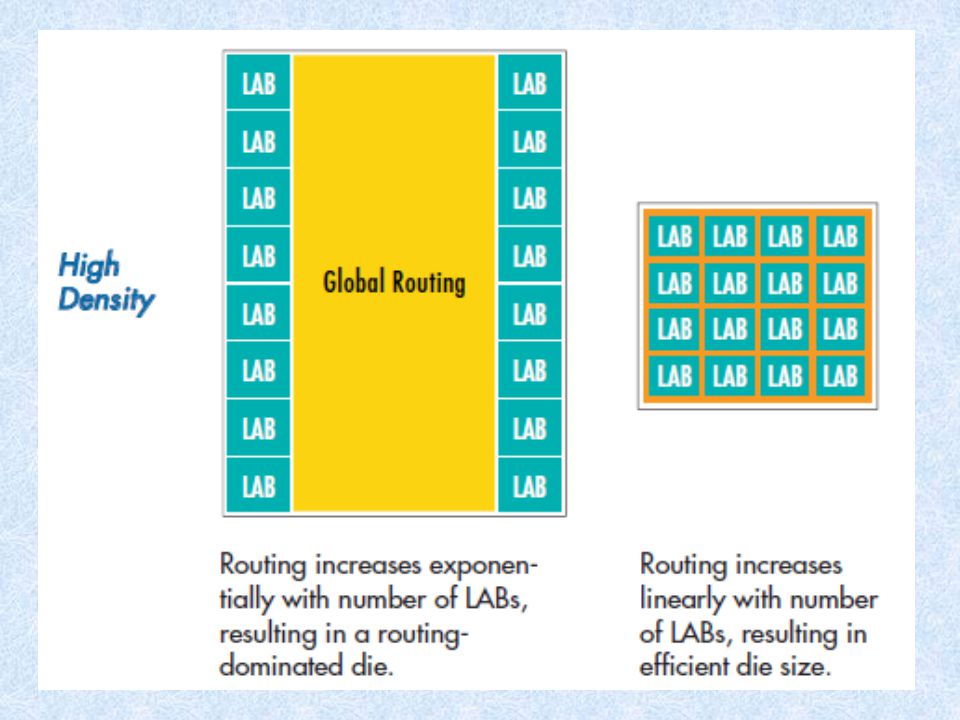
Connection between LABs

8
Difference between CPLD & FPGA
architecture Product term Look up Table configuration inner EEPROM outer EEPROM resource Rich in combination Rich in Flip-Flops density Low High Used Filed Logical control Complex algorithms Other resource - EAB,PLL security good So so

9
Global PLD Providers www.altera.com www.xilinx.com www.latticesemi.com
Inventor of CPLD,Best FPGA Inventor of FPGA,Best FPGA Inventor of ISP For G.I. and Astrionics

10
40nm、65nm、90nm、130nm High Performance FPGAs
CPLDs based on LUT General CPLDs 65nm、90nm、130nm Low Cost FPGAs Altera的芯片在国内的高校用的比较多,就像在高校里面用VHDL的人比较多一样。Altera的芯片产品比较全,目前主要的Cyclone系列(1.2.3)应用的比较广泛,Stratix( )系列一般在通信等高端领域应用比较多一些。 40nm、65nm、90nm、130nm High Performance FPGAs Low Cost FPGAs with High Speed transceiver structured ASICs Better Performance Lower Cost
应用的比较广泛,Stratix( )系列一般在通信等高端领域应用比较多一些。 40nm、65nm、90nm、130nm High Performance FPGAs. Low Cost FPGAs with High Speed transceiver. structured ASICs. Better Performance. Lower Cost.")
11
High Performance FPGAs
Virtex Series High Performance FPGAs Vitrex-5 for latest Vitrex-5 TXT,120Gbps in a single chip! Spartan Series Low Cost FPGAs Spartan-3E for latest Xilinx的公司的产品更多的被企业采用。相对于altera , Xilinx的历史更悠久一些,客户更多。Xilinx公司对芯片提供的参考设计较Altera公司提供的涉及的领域更宽,品种更多。免费使用的IP核也更多一些。Xilinx的高端FPGA在市场上占有一定的优势 CoolRunner Series CPLDs CoolRunner-II for latest

12
Anti-fuse FPGAs( Radiation protection ,perfect in security )
Flash Based FPGAs ( Inner configuration ,perfect in security ) CPLDs (EEPROM) FPGAs with ViaLink(Low power cost, perfect in security Actel公司的FPGA以反融丝类型的为主具有很好的抗辐射性能、保密性好,应用与一些特定的领域如军工和宇航 Lattice公司是ISP的发明者,主推基于Flash的FPGA,由于不需要外置配置器件,安全性较好 QuickLogic公司的FPGA也是以反融丝为主,一般用于产品的加密,目前还很难破解
 CPLDs (EEPROM) FPGAs with ViaLink(Low power cost, perfect in security. Actel公司的FPGA以反融丝类型的为主具有很好的抗辐射性能、保密性好,应用与一些特定的领域如军工和宇航. Lattice公司是ISP的发明者,主推基于Flash的FPGA,由于不需要外置配置器件,安全性较好. QuickLogic公司的FPGA也是以反融丝为主,一般用于产品的加密,目前还很难破解.")
13
Earliest access to 40-nm technology AND a low-risk path to production
Highest density, highest performance, AND lowest power

14
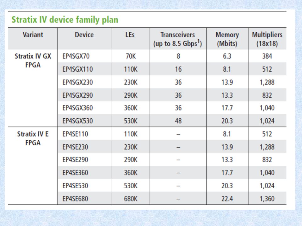
Stratix IV E FPGAs Up to 680K high-performance logic elements(LEs)
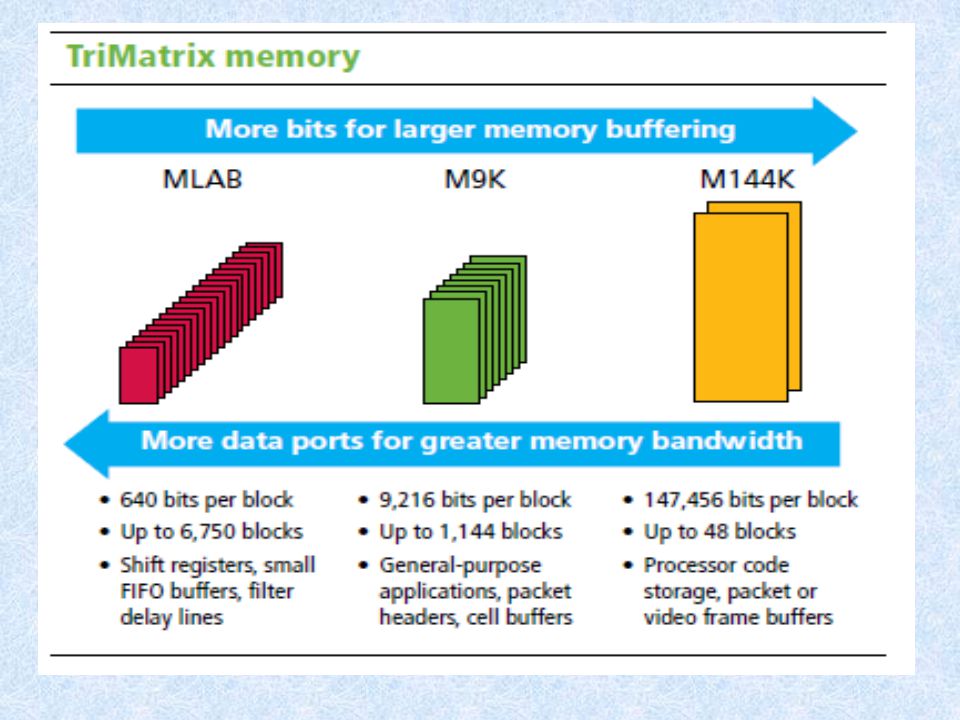
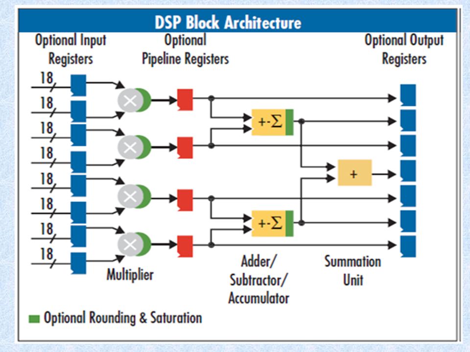
DSP blocks—with a parallel architecture and up to 1,360 embedded 18x18 multipliers running at 550 MHz, Stratix IV FPGAs deliver up to 748 GMACS of DSP performance, a level unmatched by competing devices TriMatrix memory—three memory block sizes with up to 22.4 Mbits of embedded memory running at 600 MHz An FPGA fabric that is two speed grades , or 35 percent, faster than that of the nearest competitor

15
Transceiver-based Stratix IV GX FPGAs
Up to 48 high-speed transceivers supporting data rates of up to 8.5 Gbps, including hard intellectual property (IP) protocols and signal integrity optimization blocks Up to four hard IP blocks for PCI Express (PCIe) compliant with PCIe Base Specification 2.0, 1.1, or 1.0, supporting x1, x2, x4, and x8 configurations. You’ll also have support for end-port and root-port applications. LVDS support up to 1.6 Gbps Up to four 72-bit high-speed DDR3 interfaces at 1,067 Mbps (533 MHz)
 protocols and signal integrity optimization blocks. Up to four hard IP blocks for PCI Express (PCIe) compliant with PCIe Base Specification 2.0, 1.1, or 1.0, supporting x1, x2, x4, and x8 configurations. You’ll also have support for end-port and root-port applications. LVDS support up to 1.6 Gbps. Up to four 72-bit high-speed DDR3 interfaces at 1,067 Mbps (533 MHz)")
18
adaptive logic modules(ALM) that Altera introduced in 2004 with Stratix II FPGAs. ALMs are based on our patented eight-input “fracturable” look-up table (LUT) with two dedicated adders and two registers.
 with two dedicated adders and two registers..")
21
256-bit key AES encryption with FIPS-197 certification

24
to 120,000 logic elements (LEs) and 4 Mbits embedded memory .
260-MHz multiplier performance with the highest multiplier-to-logic ratio in the industry. Robust clock management and synthesis with dynamically reconfigurable and flexible phase-locked loops (PLLs). Improved signal integrity with adjustable I/O slew rates. Support for high-speed external memory interfaces including DDR,DDR2, SDR SDRAM, and QDRII SRAM. Support for I/O standards including LVTTL, LVCMOS, SSTL, HSTL, PCI Express, LVPECL, LVDS, mini-LVDS, RSDS, PPDS.
. Improved signal integrity with adjustable I/O slew rates. Support for high-speed external memory interfaces including DDR,DDR2, SDR SDRAM, and QDRII SRAM. Support for I/O standards including LVTTL, LVCMOS, SSTL, HSTL, PCI Express, LVPECL, LVDS, mini-LVDS, RSDS, PPDS.")
27
Example—Software Defined Radio

28
Example—Software Defined Radio

29
New LUT & LE Based CPLD

34
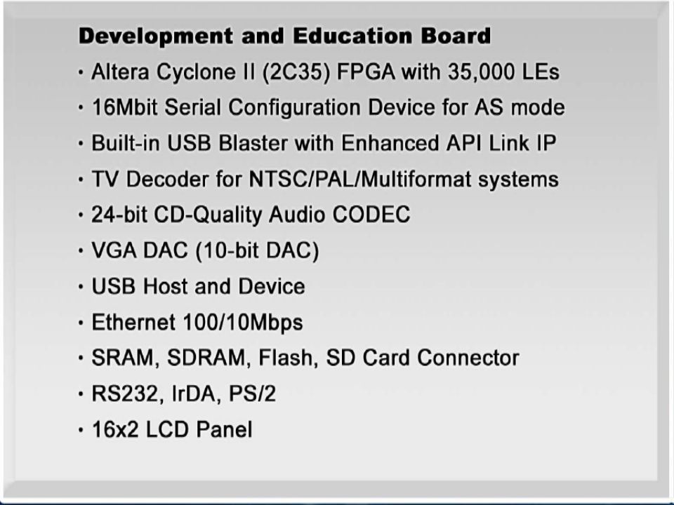
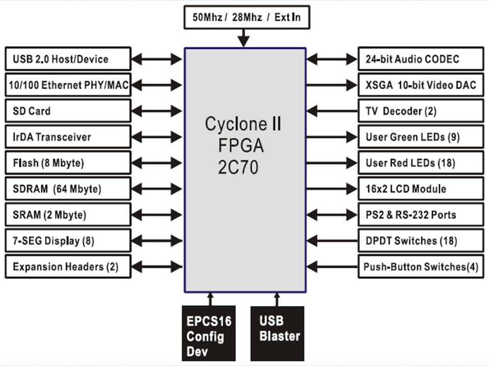
DE2 Development and Education Board
CycloneII系列最常用的 EP2C5、EP2C35、EP2C70

37
DE1 Development and Education Board

39
DE2-70 Development and Education Board

41
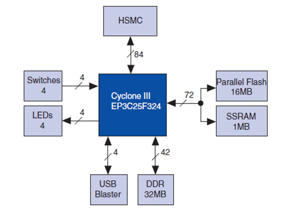
Cyclone III FPGA Starter Kit
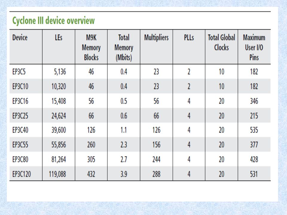
CycloneIII系列最合适的器件:EP3C5、EP3C25、EP3C80

43
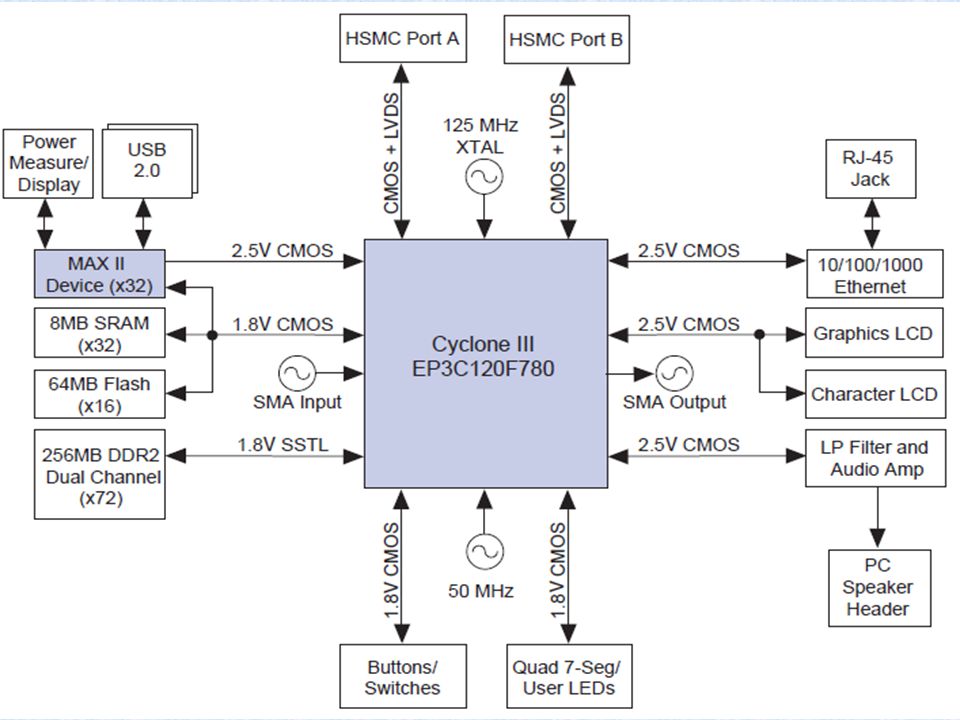
Cyclone® III Development Kit

45
Spartan-3E Starter Kit

46
Xilinx XC3S500E FPGA Xilinx XCF04 Platform Flash for storing FPGA configurations St Microelectronics M25P16 16Mbit Serial Flash Intel TE28F128 (or JS28F128) 128Mbit StrataFlash Linear Technologies Power Supplies Texas Instruments TPS75003 Triple-Supply Power Management IC SMSC LAN83C185 Ethernet PHY Micron 256Mbit DDR SDRAM
 128Mbit StrataFlash. Linear Technologies Power Supplies. Texas Instruments TPS75003 Triple-Supply Power Management IC. SMSC LAN83C185 Ethernet PHY. Micron 256Mbit DDR SDRAM.")
50
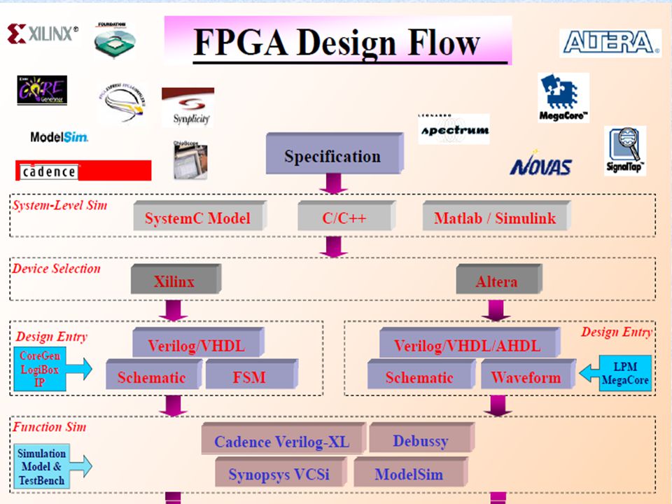
Quartus II 设计流程

51
FPGA提供了极强的灵活性,可让设计者开发出满足多种标准的产品。

52
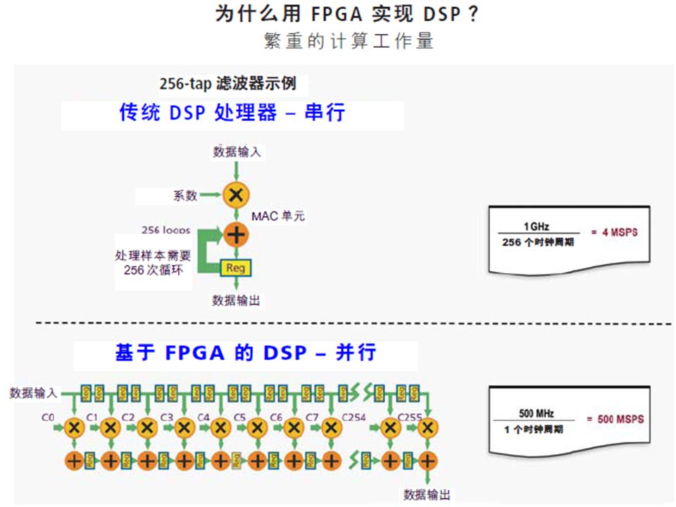
由于成本、系统功耗和面市时间等原因,许多通讯、视频和图像系统已无法简单地用现有DSP处理器来实现,FPGA尤其适合于乘法和累加(MAC)等重复性的DSP任务,最典型的就是FFT。
等重复性的DSP任务,最典型的就是FFT。")
55
复数乘法器RTL示意图

56
蝶形运算单元示意图

57
蝶形运算单元RTL示意图

58
1024点16位字长FFT耗时 TI 公司TMS320C62x: 66 μs (定点)
ADI公司TigerSharc TS101: 39 μs (浮点) Xilinx公司的FFT IP核在100M外频时钟下达到40.96 us,246MHz外频时钟下,速度达到25.49 μs (定点) Altera公司的FFT IP核在100M外频时钟下达到20.7us,在333MHz外频时钟下仅需要6.3 μs (定点)
 Xilinx公司的FFT IP核在100M外频时钟下达到40.96 us,246MHz外频时钟下,速度达到25.49 μs (定点) Altera公司的FFT IP核在100M外频时钟下达到20.7us,在333MHz外频时钟下仅需要6.3 μs (定点)")
59
r-4 DIF FFT算法在100 MHz Virtex Ⅱ上以多级串行同步流水方式 完成1 024 点、16 位复数点的块浮点FFT 处理时间为10. 2 μs
SR DIF FFT算法在100MHz Virtex II Pro 上以6级级联流水方式完成1024点、16 位复数点的块浮点FFT 处理仅需要2.56 μs 采用16块工作在550MHz 的Virtex-5 XC5VSX240T(片内1056个DSP48E Slices)的全并行结构同时处理两路信号可在1个时钟周期内完成1024点16位SR-FFT,单路处理时间小于2ns,处理延时仅为十几μs 。
的全并行结构同时处理两路信号可在1个时钟周期内完成1024点16位SR-FFT,单路处理时间小于2ns,处理延时仅为十几μs 。")
61
谢谢!

Similar presentations


![首 页 首 页 上一页 下一页 本讲内容 投影法概述三视图形成及其投影规律平面立体三视图、尺寸标注 本讲内容 复习: P25~P31 、 P84~P85 作业: P7, P8, P14[2-32(2) A3 (1:1)]](/12/3353742/big_thumb.jpg "首 页 首 页 上一页 下一页 本讲内容 投影法概述三视图形成及其投影规律平面立体三视图、尺寸标注 本讲内容 复习: P25~P31 、 P84~P85 作业: P7, P8, P14[2-32(2) A3 (1:1)]>")


 实验目的:了解关联规则在数据挖掘中的 应用,理解和掌握关联挖掘的经典算法 Apriori 算法的基本原理和执行过程并完成程 序设计。 实验内容:对给定数据集用 Apriori 算法进行 挖掘,找出其中的频繁集并生成关联规则。>")
 均迫 切需要有效地查询这些数据对象。>")

 陈辉宏. 一. 概述 信息时代的来临, 各门学科的研究方法都 有了新的发展. 计算机的介入, 为分析化学的进展提供了 一种更方便的研究方法.>")
相 互联系的质点组成的系统 研究方法: 1. 分离体法 2. 从整体考虑 把质点的三个定理推广到质点组.>")

 定子接三相电源上,绕组中流过三相对称电流,气 隙中建立基波旋转磁动势,产生基波旋转磁场,转速 为同步速 : 三相异步电动机的简单工作原理 电动机运行时的基本电磁过程: 这个同步速的气隙磁场切割 转子绕组,产生感应电动势并在 转子绕组中产生相应的电流;>")


 林佳宁 (PB03203124) 指导老师 : 秦敢 指导老师 : 秦敢.>")


 离散数学. 定理 6.2.2 群定义中的条件 ( 1 )和( 2 )可以减弱如下: ( 1 ) ’ G 中有一个元素左壹适合 1 · a=a; ( 2 ) ’ 对于任意 a ,有一个元素左逆 a -1 适 合 a -1 ·>")
