Download presentation
Presentation is loading. Please wait.

1
Kamal Banjara Rodrigo Benedetti Bob DeBorde John DeLeonardis

2
History of computer electronics The first generation : Vacuum tube The second generation : Transistors Third generation : Integrated Circuits Fourth generation : Microprocessors

3
Invention of vacuum tubes Vacuum test was an extremely important step in the advancement of computers. Very important characteristics is that they can convert amplify the signals Switch on and off electricity But; They are slow, expensive and need thousands in number to operate They got heated very quickly Whats the remedy then? http://www.computermuseum.li/Testpage/UNIVAC- VacuumTube.htm

4
Transistors New Device that quickly replaced the vacuum tubes Why? Because - can be used to relay and switch signals - faster, more reliable, smaller in size, and cheaper to build - gave off virtually no heat compared to vacuum tube Officially announce the era of silicon - Silicon is the main element in transistors http://chinaimportexport.wikispaces.com/file/view/Darlingt on_Transistors__TO_220___126_.jpg/33663811/Darlington_T ransistors__TO_220___126_.jpg

5
Silicon the first Semiconductor element Introduction of silicon is a breakthrough in modern electronics Transistors were followed by integrated circuits and microprocessors Now, our computers are smaller and faster and reliable Electronic structure of silicon atom:–10 core electrons (tightly bound)–4 valence electrons (loosely bound, responsible for most of the chemical properties http://en.wikipedia.org/wiki/File:Silicon-unit-cell-3D- balls.png
–4 valence electrons (loosely bound, responsible for most of the chemical properties balls.png")
6
What is a Semiconductor?

7
Semiconductor Diode and transistors are the most common example of semiconductor devices Silicon, Germanium, Gallium Arsenide Carbon are the Semiconductor substances Among all these Silicon is widely used because of its low material cost, relatively simple processing and useful temperature range Other are not as useful as silicon but when they are alloyed with Silicon, they can be used in making very useful devices. E.g. SiGe devices http://images.businessweek.com/ss/07/02/0201_carly le_deals/image/freescale_semiconductor.jpg

8
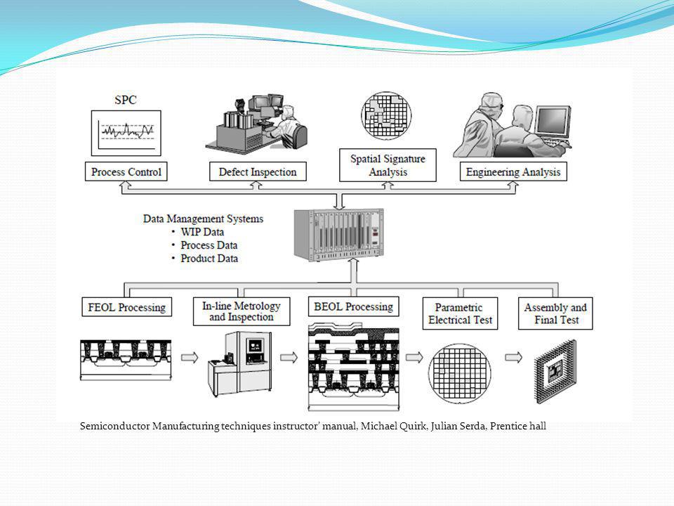
Semiconductor Manufacturing Processes Design Wafer Preparation Front-end Processes Photolithography Etch Cleaning Thin Films Ion Implantation Planarization Test and Assembly Thin Films Photo- lithography Cleaning Front-End Processes Etch Ion Implantation Planarization Test & Assembly Design Wafer Preparation NSF/SRC Engineering Research Center for Environmentally Benign Semiconductor Manufacturing, Conrad T. Sorenson, Praxair, Inc.

9
Design Designing the transistor architecture and establishing design rules, Designing basic circuit elements that can be used as building blocks for more complex circuits, Simulating the complex circuit so that undesired properties can be eliminated, and Preparing the pattern for lithography. www.webuyics.com/electronic-components.htm

10
Wafer Preparation Polysilicon Refining: Si Refining: SiO 2 + 2 C Si + 2 CO Si Purification: Si + 3 HCl HSiCl 3 + H 2 Crystal Pulling: Czochralski process Time: 18 to 24 hours Temperature: >1,300 degrees C Pressure: 20 Torr Pulling: ~0.7 mm/min for 300mm ingots www.intel.com/.../releases /2006/20060125comp.htm Semiconductor Manufacturing techniques instructor manual, Michael Quirk, Julian Serda, Prentice hall

11
Wafer Slicing & Polishing: The crystal ingot is then cut by a diamond saw blade cuts the ingot into thin wafers and ground to a uniform diameter. Chemically and physically polished. Semiconductor Manufacturing techniques instructor manual, Michael Quirk, Julian Serda, Prentice hall

12
Front-End Processes Thermal Oxidation Silicon Nitride Deposition Low Pressure Chemical Vapor Deposition (LPCVD) Polysilicon Deposition Low Pressure Chemical Vapor Deposition (LPCVD) Annealing Semiconductor Manufacturing techniques instructor manual, Michael Quirk, Julian Serda, Prentice hall
 Polysilicon Deposition Low Pressure Chemical Vapor Deposition (LPCVD) Annealing Semiconductor Manufacturing techniques instructor manual, Michael Quirk, Julian Serda, Prentice hall")
13
Photolithography The image of the circuit pattern is transferred to the wafer Photoresist Coating Processes Exposure Processes light Short wavelength for small devices uv NSF/SRC Engineering Research Center for Environmentally Benign Semiconductor Manufacturing, Conrad T. Sorenson, Praxair, Inc.

14
Ion Implantation This process is better known as doping. Not a new layer Ion implanter Creation of regions : Insulating, or p-type conducting, or n-type, https://fys.kuleuven.be/vsm/nano/news.php

15
ETCHING Removal of photoresist. Heat treatment Chemical or plasma Semiconductor Manufacturing techniques instructor manual, Michael Quirk, Julian Serda, Prentice hall

16
Cleaning and thin films There are three major types of cleans used: Critical cleans, photoresist strips, and pre-deposition cleans Thing films : Chemical Vapor Deposition (CVD) Dielectric CVD Tungsten Physical Vapor Deposition (PVD) http://cientifica.eu/blog/page/20/?s=cientifica
 Dielectric CVD Tungsten Physical Vapor Deposition (PVD) s=cientifica")
17
Planarization, test and assembly Denser interconnection layers. Test and assembly operation are performed out of the cleanroom wafer fab. In these operations, chips are tested, put into packages, then retested. Semiconductor Manufacturing techniques instructor manual, Michael Quirk, Julian Serda, Prentice hall

20
Alvin H. Romang and James J. Watkins July, 2009

21
Motivation Supercritical Fluids (SCF) Offers advantages of liquid and gaseous states Solubility similar to liquid phase Mass transfer properties of a vapor Allows for additional precursors and reagents http://www.che.tohoku.ac.jp/~scf/about/souzu-E.gif
 Offers advantages of liquid and gaseous states Solubility similar to liquid phase Mass transfer properties of a vapor Allows for additional precursors and reagents")
22
Applications: Metal/Metal Oxide Deposition Chemical Vapor Deposition (CVD) Vapor Phase Low Precursor Volatility Low Concentration Kinetics limited by mass transport Non-uniform deposition May require several steps http://itech.dickinson.edu/chemistry/wp-content/uploads/2008/04/pg02.jpg
 Vapor Phase Low Precursor Volatility Low Concentration Kinetics limited by mass transport Non-uniform deposition May require several steps")
23
Applications: Metal/Metal Oxide Deposition Atomic Layer Deposition (ALD) Vapor phase Provides Good step coverage Difficult to produce thick Layers http://lsm.rutgers.edu/images/facility_ALD01_tm.gif
 Vapor phase Provides Good step coverage Difficult to produce thick Layers")
24
Applications: Metal/Metal Oxide Deposition Supercritical Fluid Deposition (SFD) Uses supercritical fluid Low viscosity Rapid diffusion Low surface tension Higher precursor concentrations Supercritical Fluids for the Fabrication of Semiconductor Devices: Emerging or Missed Opportunities. Alvin H. Romang and James J. Watkins. July, 2009

25
Precursor concentration Supercritical Fluids for the Fabrication of Semiconductor Devices: Emerging or Missed Opportunities. Alvin H. Romang and James J. Watkins. July, 2009

26
Cu Deposition Supercritical Fluids for the Fabrication of Semiconductor Devices: Emerging or Missed Opportunities. Alvin H. Romang and James J. Watkins. July, 2009

27
Advantages of SFD No fluorinated precursors High Purity Supercritical Fluids for the Fabrication of Semiconductor Devices: Emerging or Missed Opportunities. Alvin H. Romang and James J. Watkins. July, 2009

28
Plasmonics for Improved Photovotaic Devices Nature Materials 9, 205 - 213 (2010) Harry A. Atwater & Albert Polman. http://www.crunchgear.com/wp-content/uploads/2008/07/solar_panel.jpg

29
Solar cells – The Basics http://www.homesolarpowersystems.org/how-solar-panels-work e-e-

30
Unfortunately… In 2006, the most cutting edge, super-efficient solar cell had efficiencies of 40.7% Average efficiency was between 12-18% 1

31
The current method to improve the light absorbance is by reflecting light back through the solar cell. Pyramidal shapes increase the scattering of light over the cell. ~GOOD~ They also contribute to the thickness of the device. ~BAD~ Semiconductor

32
Plasmonic Light-trapping 3 methods…. Light scatteringPlasmon excitationPlanar plasmon propagation

33
Nanotechnology at wok By using nanoparticles of gold or silver, common enough elements, one can reduce the thickness of solar cells while keeping, sometimes improving, the efficiency. Most of the cost of solar cells is due to the materials, and some semiconductors like Tellurium and Indium are not used because of the cost. 100 nm 200 µm

34
Customized to suit your needs Size and shape have different effects. 150 nm Ag particles have a large albedo, reflecting 95% of light as radiation. 5-20 nm particles work like antennas by enhancing the local field of nearby semiconductors.

35
Finished Product Silver film on Si wafer. Silver nanoparticles evaporated through template. Si wafer with metal nanopattern.

36
Implications of Research Photovoltaic Devices Lower production cost Use of Scarce Materials Increased solar production http://www.nature.com/nmat/journal/v9/n3/fig_tab/nmat2629_T1.html

37
Implications of Research Supercritical Fluids Faster component production High Purity Greater number of reagents More powerful computer chips http://www.bcgsafety.com/media/images/semiconductor.jpghttp://www.automotive-res.com/EX/11-16-23/semiconductor-560x420.jpg

38
Controversy Semiconductors are an established industry Resistance to change New Processes/Technology may be obsolete http://www.semi-gas.com/images/operators1p.jpg http://img.tomshardware.com/us/2007/04/25/semiconductor_production_101/wafer-test.jpg

39
Additional Research Testing new reagents with SCF Advanced Plasmonic Solar Cells http://www.nature.com/nmat/journal/v9/n3/fig_tab/nmat2629_F6.html

40
Questions

41
References http://www.howstuffworks.com/solar-cell.htm Semiconductor Manufacturing techniques instructor manual, Michael Quirk, Julian Serda, Prentice hall

42
Rebuttal Group from U1 Semiconductor Manufacturing Techniques

43
Review of Some of the Comments All of the group members were leaning against the podium or sitting down during another members presentation. We agree that maintaining a good posture is important, but as Dr. Seminario commented, it is the message that the group conveys what's relevant. The comments on the overall work were good critiques, but we apologize for the big difference in the oral presentation skills of some of the speakers. Mastering this skills by foreign students is a process that involve time and more practice and we are aware of that. It was not lack of preparation or knowledge about the topic. Some of the comments also pointed out that more information could have been given, but we think the information given was sufficient and non repetitive, long enough that extended our presentation for more than 40 minutes. http://www.artskills.com/parents_o ral_presentations.php

44
Rebuttal (cont) We DO agree that we should have really scoured our presentation for mistakes in spelling and capitalization errors. These things can really take away from the overall message and certainly looks unprofessional. Many students wanted more information but what they dont realize is how hard it was to relate semiconductors to nano-technology. If we had spent 30 minutes going over how solar cells work and the exact processes of manufacturing semiconductors, the students would then complain that the presentation did not adhere to the course material. I hope you see the dilemma. We tried to do our best to give a general overview of what a semiconductor is and how it is made, any additional information seemed unnecessary for us to present. For instance– solar cells are so inefficient because silicon has a band gap of about 1.1 eV. So any light energy that has at least 1.1 eV will move an electron, but if there is more than 1.1, the rest is converted to heat instead of electricity. This is one of many factors that causes solar cells to be so inefficient. This kind of information, while interesting, does not really apply to how nano- technology can help improve photovoltaic devices. If our presentation had been about semiconductors in general we certainly would have spent more time discussing their properties.

45
By Group U2: -Kyle Demel -Kyle Demel -Keaton Hamm -Keaton Hamm -Bryan Holekamp -Bryan Holekamp -Rachael Houk -Rachael Houk http://www.claimsmag.com/Issues/2009/DECEMBER-2009/PublishingImages/NanotechnologyImage.jpg Review of Group U1s Presentation-

46
The presenters did really well at: Background – The speakers did a good job explaining all the pertinent information needed to comprehend the topic of semiconductors. They began with a brief history of semiconductor technology, discussing the transition from vacuum tubes all the way through integrated processors. They also discussed the material science that allows certain elements to behave as they do. The manufacturing process was very thorough, and the follow-up video was a nice touch that added value to the overall presentation. Articles – The group chose to present two articles, a nice improvement over the one article reports that most groups gave. One article discussed using supercritical fluids for semiconductor fabrication, and the other article discussed using plasmonics to improve photovoltaic devices. Although our group is still not certain what plasmonics are, we enjoyed hearing the graduate students and Dr. Seminario share their knowledge on the subject. Graphics – The consistent use of graphics on all the slides was a nice feature. The graphics helped to clearly demonstrate the information being presented. Also, all the graphics were appropriately sized. http://www.treehugger.com/files/2008/05/nano-vent-skin.php

47
The group could improve at: Oral presentation – Some group members were really fantastic speakers while a few of them should practice more. Some key things to work on include maintaining better eye contact with the audience, speaking clearly and slowly, adding pauses and changing tone of voice for greater emphasis, and using less filler words. All of the group members were leaning against the podium or sitting down during another members presentation. The group needs to maintain better body posture throughout the presentation, which will also make the current speaker seem more interesting. Proofread – Make sure to proofread the slides before posting online, especially the titles. Ex. slide 33 – Nanotechnology at wok The group did a good job discussing the future research and the controversy of the future research, but they did not back these slides up with any additional articles. For controversy, they could have cited/summarized an articles that talked about the difficulties in implementing new technologies in the semi- conductor industry. For additional research, they could have assembled a montage of other articles that are researching semiconductor improvements. http://etfdb.com/wp-content/uploads/2009/11/Semiconductor-ETFs-Are-Similar-But-Different-300x231.jpg

48
Group 3: Krista Melish James Kancewick Phillip Keller Mike Jones Undergrad Review for Group U1 Semiconductor Manufacturing Techniques

49
Presentation Review: Ugrad #1 Presentation ReviewMaterial Review Introduction Effectively introduced the audience to the subject Included short history of semiconductors, definition, mechanical explanation, and a thorough explanation of current manufacturing techniques that were the focus of the research to improve with supercritical fluids Oral Communication Verbal distractors are always present in every presentation, but they did not detract from presenting the material. Volume, tone, clarity of speech, posture, and body movement were all sufficient as to not interfere Capitalization Errors All words in titles should be capitalized, several slides at the beginning had this mistake. Super Critical Fluids paper Well presented and explained, but the research material itself isnt nanotechnology. It is used to create nanoelectronics, but the research itself doesnt directly apply. Still interesting though. Plasmonics for Improved Photovoltaics Research material directly applies to nanotech Well explained for such a high level confusing topic. Appreciate humility in presenting, but it is never good to straight up say you dont understand something. Instead, research it before hand, or state that the complexity is not within the scope of the course. Further Research Suggestions were not very well elaborated Suggest a topic, and then say how you might go about accomplishing it and how it what benefits you would be after. Suggestion: Further investigate the Plasmonic effect of nanoparticles by using a mixture of silver and gold with the hopes of finding new behaviors due to the interactions of the different materials.

50
Semiconductor Manufacturing Techniques (U1) Group U4 Review
 Group U4 Review")
51
Introduction Pros: Introduction part was excellent in including basic theory behind semiconductor and how they work. Critical comparison and discussion of history of electronics and semiconductors (vacuum tubes, Transistors, etc). Cons: Why was the introduction of silicon a breakthrough in modern electronics ? Explain chemical properties more. Comparison of most used semiconducting materials, why are some preferred over others ? * Figures taken from U1 presentation
. Cons: Why was the introduction of silicon a breakthrough in modern electronics . Explain chemical properties more. Comparison of most used semiconducting materials, why are some preferred over others . * Figures taken from U1 presentation.")
52
Manufacturing Processes Thin Films Photo- lithography Cleaning Front-End Processes Etch Ion Implantation Planarization Test & Assembly Design Wafer Preparation * Figures taken from U1 presentation Pros: Different stages of manufacturing semiconductors were effectively discussed and explained with the aid of visual figures. Overall figure shown to the right was excellent in better understanding the complete process and how each stage is connected to the other (i.e. Wafer Preparation, reaction involved and Czochralski process conditions (Temperature, pressure, etc). Cons: Explain more about Front-End Processes, what are the chemical reaction involved in thermal oxidation ? Explain the figure showed on that section. How are n-type and p-type regions made in ion implantations stage ? Why a donor ion is implanted ?
. Cons: Explain more about Front-End Processes, what are the chemical reaction involved in thermal oxidation . Explain the figure showed on that section. How are n-type and p-type regions made in ion implantations stage . Why a donor ion is implanted .")
53
Researched paper and conclusion * Figures taken from U1 presentation Pros: Excellent use of figures in explaining Cu deposition in Supercritical Fluid Deposition (SFD) Mentioned motivation and applications of using SCF in the manufacturing of semiconductors. Comparison of different metals used and how they effect fluorinated precursors and purity. Cons: super-efficient solar cell had efficiencies of 40.7%, explain more why efficiency is low ? Discuss more what kind of further research needed for advanced plasmonic solar cells.

54
Oral Skills Group members were all very knowledgeable of subject. All presenters spoke in a clear tone and showed confidence. All members of the group answered questions effectively. Transition between presenters was smooth and quick.

55
Review of Group U1 by Group U5

56
Speakers had good oral presenting skills. Communication of information was well thought out and could tell that it was practiced. Nice visually attractive slides. Very good balance of figures and text. All pictures served a purpose in the slide they were presented.

57
Introduction was excellent. Liked the way they introduced semiconductors and taught about how they worked in the intro. Informative and attention capturing. Good choice of papers for the topic at hand. Interesting and relevant.

58
Presented by: Group U1 Critiqued by: Group U6 Semiconductor Manufacturing Techniques http://www.ceilcoteapc.com.sg/images/semiconductor.gif

59
Critique: Oral Presentation & Slides Slides were easy to read Good background and good size text Good transition between slides Would have liked to see slides thought out a little more (paid a little more attention to detail) The use of illustrations complimented the text – would have liked to see more use of graphics though The illustrations were cited and found on almost every page An outline slide would have been helpful in letting the audience know what to expect Excellent flow of topics in the introduction The first and second speaker did not maintain as much eye contact as the third and fourth speakers. Also, the first two speakers seemed to waiver when talking to the audience- this problem would have been solved if they practiced more Liked that group members dressed up for presentation Enjoyed the snacks provided – thanks! http://www.gourmet.com/images/recipes/ 2000/08/rs_icepops608.jpg http://www.beatsworking.tv/tristan/eyecontact.jpg

60
Critique – Technical Content Manufacturing techniques of semiconductors explained well Presenters took audience through step-by-step process Choice of research papers seemed relevant to topic discussed Supercritical fluids can be useful for additional precursors and reagents Can use nanotechnology to reduce thickness of solar cells and maybe improve efficiency Further research on this topic could potentially revolutionize manufacturing techniques – however, very lukewarm reception by industry The group could have presented additional research possibilities instead of just two Would have liked to see potential long term impact of the research presented http://www.inhabitat.com/wp-content/uploads/nanosys_solar.jpg http://www.che.tohoku.ac.jp/~scf/about/souzu-E.gif https://fys.kuleuven.be/vsm/nano/news.php http://www.nature.com/nmat/journal/v9/n3/fig_tab/nmat2629_F6.html

61
Review for U1 Jung Hwan Woo

62
Explanation as to why non-fluorinated process in SFD is advantageous may be needed. What type of materials can SFD deposit? Which process can SFD substitute in the current silicon processing? Does plasmonic solar cell use transparent film unlike the light-absorbing surface on the current solar cells? Then, how are the photons captured?

Similar presentations


. Diffusion Process The process of materials move from high concentration regions to low concentration regions,>")


>")
 Electrodes (ode)>")


