Download presentation
Presentation is loading. Please wait.

1
Timing & process Instruction:-It is a command which direct the processor to execute certain task. Ex:- MOV A,B I.Op-code: what operation the MP will perform. Ex:-MOV II.Operand:- On which data the MP will operated on. Ex:- A,B

2
Instruction cycle:- The time taken to complete the execution of one instruction. Machine Cycle:- The time taken to complete the execution of one machine. Each reference of the MP to its peripherals is one machine cycle.

3
Types of Machine cycle Opcode fetch m/c (6T) Opcode fetch m/c (4T) Memory read m/c (3T) Memory write m/c (3T) I/O read m/c -3T I/O write m/c -3T Bus Idle m/c - Undefined
 Opcode fetch m/c (4T) Memory read m/c (3T) Memory write m/c (3T) I/O read m/c -3T I/O write m/c -3T Bus Idle m/c - Undefined")
4
Opcode fetch machine cycle of 8085 : Each instruction of the processor has one byte opcode. The opcodes are stored in memory. So, the processor executes the opcode fetch machine cycle to fetch the opcode from memory. Hence, every instruction starts with opcode fetch machine cycle. The time taken by the processor to execute the opcode fetch cycle is 4T. In this time, the first, 3 T-states are used for fetching the opcode from memory and the remaining T-states are used for internal operations by the processor.

6
Memory Read Machine Cycle of 8085: The memory read machine cycle is executed by the processor to read a data byte from memory. The processor takes 3T states to execute this cycle. The instructions which have more than one byte word size will use the machine cycle after the opcode fetch machine cycle.

8
Memory Write Machine Cycle The memory write machine cycle is executed by the processor to write a data byte in a memory location. The processor takes, 3T states to execute this machine cycle.

10
I/O Read Cycle of 8085: The I/O Read cycle is executed by the processor to read a data byte from I/O port or from the peripheral, which is I/O, mapped in the system. The processor takes 3T states to execute this machine cycle. The IN instruction uses this machine cycle during the execution.

12
I/O Write Cycle of 8085: The I/O write machine cycle is executed by the processor to write a data byte in the I/O port or to a peripheral, which is I/O, mapped in the system. The processor takes, 3T states to execute this machine cycle.

14
Bus Idle machine cycle

15
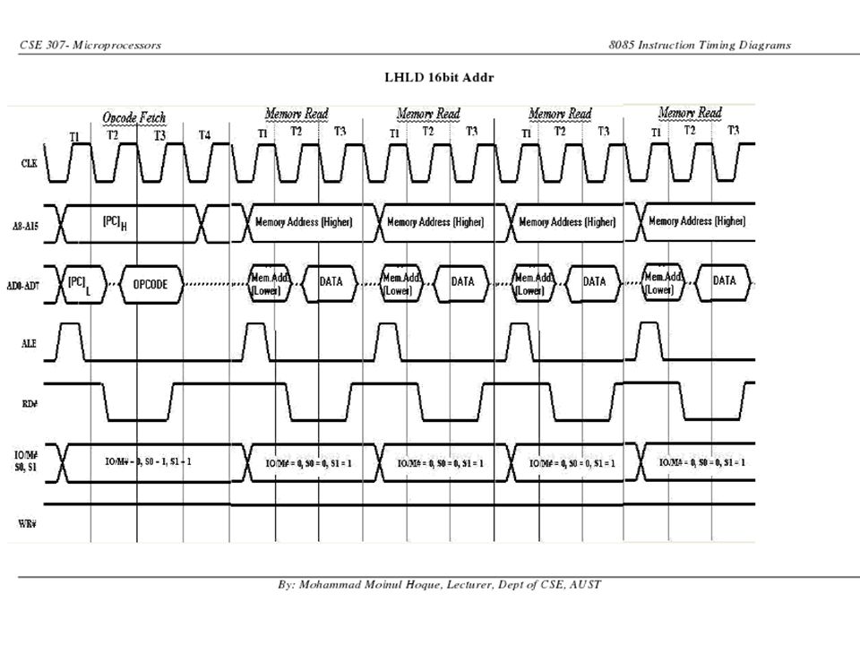
Timing diagram for INR M Fetching the Opcode 34H from the memory 4105H. (OF cycle) Let the memory address (M) be 4250H. (MR cycle -To read Memory address and data) Let the content of that memory is 12H. Increment the memory content from 12H to 13H. (MW machine cycle)
 Let the memory address (M) be 4250H. (MR cycle -To read Memory address and data) Let the content of that memory is 12H. Increment the memory content from 12H to 13H. (MW machine cycle).")
17
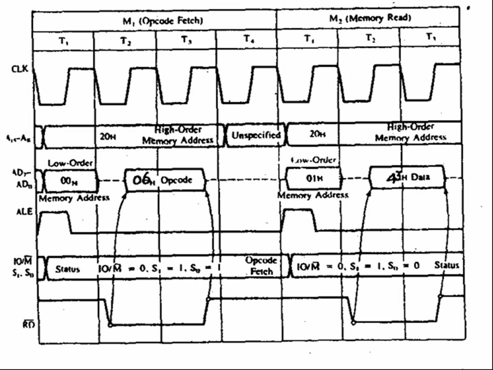
Timing diagram for MVI B, 43H Fetching the Opcode 06H from the memory 2000H. (OF machine cycle) Read (move) the data 43H from memory 2001H. (memory read)
 Read (move) the data 43H from memory 2001H. (memory read).")
19
Timing diagram for STA 526AH STA means Store Accumulator -The contents of the accumulator is stored in the specified address(526A). The opcode of the STA instruction is said to be 32H. It is fetched from the memory 41FFH(see fig). - OF machine cycle Then the lower order memory address is read(6A). - Memory Read Machine Cycle Read the higher order memory address (52).- Memory Read Machine Cycle The combination of both the addresses are considered and the content from accumulator is written in 526A. - Memory Write Machine Cycle Assume the memory address for the instruction and let the content of accumulator is C7H. So, C7H from accumulator is now stored in 526A.
. - OF machine cycle Then the lower order memory address is read(6A). - Memory Read Machine Cycle Read the higher order memory address (52).- Memory Read Machine Cycle The combination of both the addresses are considered and the content from accumulator is written in 526A. - Memory Write Machine Cycle Assume the memory address for the instruction and let the content of accumulator is C7H. So, C7H from accumulator is now stored in 526A..")
22
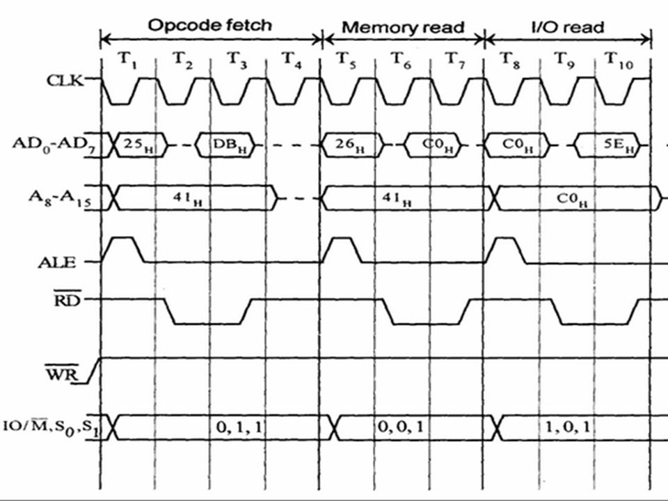
Timing diagram for IN C0H. Fetching the Opcode DBH from the memory 4125H. Read the port address C0H from 4126H. Read the content of port C0H and send it to the accumulator. Let the content of port is 5EH.

32
SIM and RIM for interrupts: The 8085 provide additional masking facility for RST 7.5, RST 6.5 and RST 5.5 using SIM instruction. The status of these interrupts can be read by executing RIM instruction. The masking or unmasking of RST 7.5, RST 6.5 and RST 5.5 interrupts can be performed by moving an 8-bit data to accumulator and then executing SIM instruction. The format of the 8-bit data is shown below.

34
The status of pending interrupts can be read from accumulator after executing RIM instruction. When RIM instruction is executed an 8-bit data is loaded in accumulator, which can be interpreted as shown in fig.

Similar presentations


 Example of program execution 1. instruction B25 8 Op-code B means to change the value of the program counter if the contents of the indicated register.>")


 1 Prepared By: Associate Prof. Dr Masri Ayob.>")


 Program Execution. 2 In the CPU we have CU and ALU, in CU there are two special purpose registers: 1. Instruction Register 2. Program Counter.>")


