Download presentation
Presentation is loading. Please wait.

1
CSF Chap B Functional components of computer designs Basic logic gates

10
The 2 level AND-OR logic circuit is a standard structure for combinational logic circuits that do not have “states” Example of a programmed logic array PLA

11
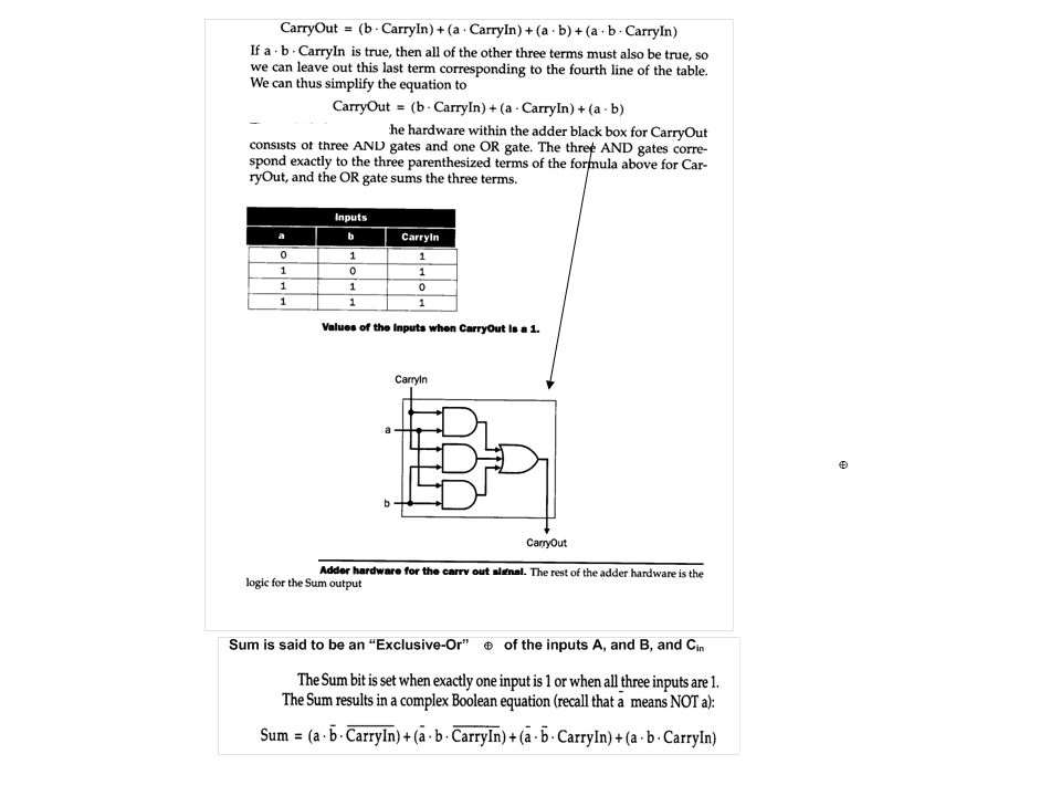
This logic circuit can be viewed as a primitive 1-bit slice of an arithmetic-logic unit (ALU). It can before logic operations: AND and OR; and it can perform an arithmetic operation: Addition

13
A more “powerful” 1-bit slice of an ALU

15
Overflow Detection: Example: two 32 bit numbers are added, and the sum does not fit in 32 bits.

20
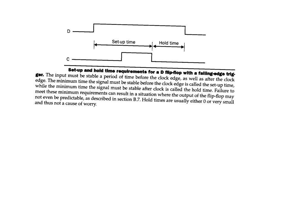
C is the clock D is the Data input (1 bit) When C=1, D is stored on Q
 When C=1, D is stored on Q")
25
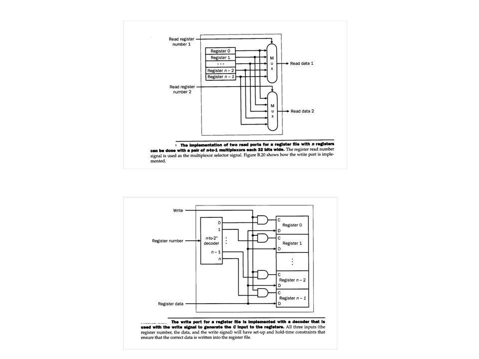
A register is essentially a small memory usually holding words (operands, memory addresses, instructions, and control flags). A set of registers is called a register file. The register file can be directly accessed by the arithmetic logic unit (ALU) when executing an instruction. The memory cells in a register file are “fast” so as to have access (reads and writes) that support the functional operating time of the logic circuits in the ALU.
 when executing an instruction. The memory cells in a register file are fast so as to have access (reads and writes) that support the functional operating time of the logic circuits in the ALU..")
29
Where are the 8 bits (one byte) of an addressable memory byte stored?
 of an addressable memory byte stored")
30
Each one of the 8 bits of each byte is stored in a different one of the 512x64 SRAMs. Why? Doing this means that a single SRAM failure effects only one bit of each byte as opposed to an entire byte. So by storing redundant bits with each byte, a bit error could be detected and even corrected.

32
Note that for any 7 bit word (for example, 0000000), there is no single bit flip that changes that word into any of the other 7 bit words. A bit error in a memory word can be detected/corrected by appending extra bits Large memories can have flawed bits (for example, a bit stuck- at-0 or stuck- at-1). To detect stuck bits, extra redundant bits can be stored. Assume a data word has 4 bits. Then 3 extra bits can be appended so that any single bit error can be corrected.
. To detect stuck bits, extra redundant bits can be stored. Assume a data word has 4 bits. Then 3 extra bits can be appended so that any single bit error can be corrected..")
33
Red and Green traffic light states only (no yellow light.

34
The current state corresponds to a set of D-FF states. For the traffic light controller, there are only 2 states: NSgreen/EWred And EWgreen/NSred A single FF can represent the current state

36
Problem: Show a state Transition diagram for a traffic light controller where a counter/timer is used to determine a period of time during which the TL stays green in each direction. It is also assumed that a yellow light stays on for a fixed amount of time as determined by a counter/timer after a car is detected. Problem

37
INC=Increment INC causes a transition from one state to next D flipflop is master/slave. Important! 2x1 Mux Reset forces transition to 0 state Operates as a 1-bit oscillator: Q flips from 0 to 1 to 0 to 1 to ….. Problem: What are the modules and the connections between them to implement modulo 8 counter? What about a module 2 R counter?

38
1 bit Arithmetic Logic Unit (ALU) module (2 types) Overflow Detection
 module (2 types) Overflow Detection")
40
Note that the carry-outs “ripple” forward to the higher order bits. (Figure 3.2). Instead of having the delay of the carry ripple, it’s possible to look ahead to determine the carry-out bits.
. Instead of having the delay of the carry ripple, it’s possible to look ahead to determine the carry-out bits..")
41
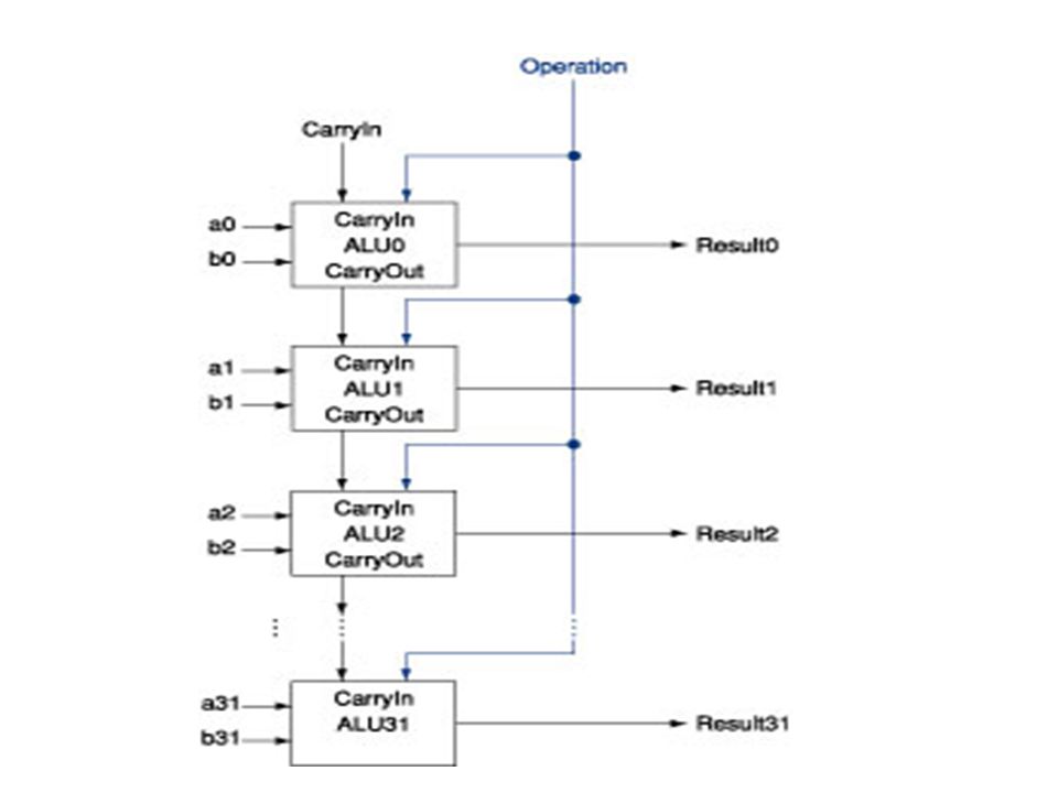
The add operation on the ALU is “slow” because a carry- out of the bit 0 add might have to “ripple” all the way to the bit 31 add before the 32 bit sum can be computed.

44
All good things must come to an end………. If we continued as above, C31 would be a “big circuit”

Similar presentations


 Felix Noble Mirayma V. Rodriguez Agnes Velez University of Puerto Rico Mayagüez Campus Mayagüez, Puerto.>")


