Download presentation
Presentation is loading. Please wait.

1
발표자 : 이재신 발표 일시 : 2003. 12. 29

2
Chapter 2 Hardware Fundamentals for the Software Engineer The embedded-systems software engineer must often understand the hardware in order to write correct software; must install the software on the hardware; must sometimes figure out whether a problem is caused by a software bug or by something wrong in the hardware; may even be responsible for reading the hardware schematic diagram and suggesting corrections

3
Contents 2.1 Terminology 2.2 Gates 2.3 A Few Other Basic Considerations. 2.4 Timing Diagrams 2.5 Memory

4
2.1 Terminology Most digital electronic circuits today are built with semiconductor parts called chips

5
PCB - Printed circuit board Schematic diagram - Drawing that show each part needed in the circuit and the interconnections needed among them Most digital circuits use just two voltages - 0 volts : “low”, “GND”, “VSS” (MOS) - Either 3 volts or 5 volts : “high”, “VCC”, “VDD” (MOS) Most digital circuit contains many signals whose purposes are to indicate various conditions - “get data from this memory chip” 2.1 Terminology (cont)
 - Either 3 volts or 5 volts : high , VCC , VDD (MOS) Most digital circuit contains many signals whose purposes are to indicate various conditions - get data from this memory chip 2.1 Terminology (cont)")
6
Assign a name to each signal in the circuit - Data signal : D0, D1, D2 - Address signal : A0, A1, A2 - “read from memory now” : MEMREAD Active low : MEMREAD*, MEMREAD, MEMREAD/ Input : Sense the voltage level Output : Control the voltage level → drive the signal Flouting : No part on the circuit is driving a signal Bus fight : One output part tries to drive one way and the other tries to drive the other 2.1 Terminology (cont)
")
7
2.2 Gates Inverters, AND Gates, and OR Gates AND Gate ( Input 1 · Input 2 = Output) Input 1Input 2Output High Low HighLow
 Input 1Input 2Output High Low HighLow")
8
OR Gate ( Input 1 + Input 2 = Output) XOR Gate ( Input 1 Input 2 = Output) Input 1Input 2Output High Low HighLowHigh LowHigh Low Input 1Input 2Output High LowHigh LowHigh Low 2.2 Gates (cont)
 XOR Gate ( Input 1 Input 2 = Output) Input 1Input 2Output High Low HighLowHigh LowHigh Low Input 1Input 2Output High LowHigh LowHigh Low 2.2 Gates (cont)")
9
The Bubble Used to indicate that an input or an output is inverted Inverter ( Input = Output) 2.2 Gates (cont)
 2.2 Gates (cont)")
10
NAND Gate ( (Input 1 · Input 2) = Output) OR Gate with Negated Input ( Input 1 + Input 2 = Output) 2.2 Gates (cont) Input 1Input 2Output High Low HighLowHigh LowHigh Low High Input 1Input 2Output High Low HighLowHigh LowHigh Low High
 = Output) OR Gate with Negated Input ( Input 1 + Input 2 = Output) 2.2 Gates (cont) Input 1Input 2Output High Low HighLowHigh LowHigh Low High Input 1Input 2Output High Low HighLowHigh LowHigh Low High")
11
Another Inverter ( Input = Output) Another Circuit 2.2 Gates (cont)
 Another Circuit 2.2 Gates (cont)")
12
2.3 A Few Other Basic Considerations Power and Decoupling Each chip in any circuit has a power pin (VCC) and a ground pin (GND) but usually do not appear an circuit schematic For example, 7400 has 14 pins, of which 2 are VCC and ground pins, and remaining 12 pins are 12 input/output signals
 and a ground pin (GND) but usually do not appear an circuit schematic For example, 7400 has 14 pins, of which 2 are VCC and ground pins, and remaining 12 pins are 12 input/output signals")
13
2.3 A Few Other Basic Considerations (cont) Decoupling capacitor - Decoupling capacitor is connected between VCC and ground pin, thus preventing momentary voltage drop
 Decoupling capacitor - Decoupling capacitor is connected between VCC and ground pin, thus preventing momentary voltage drop")
14
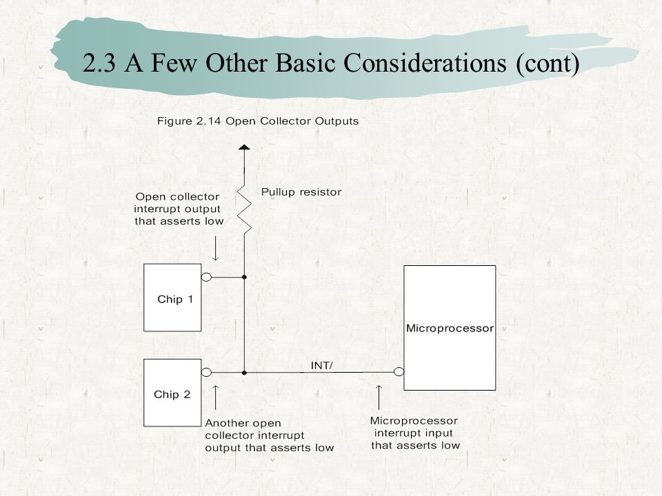
Open collector and tri-stating Outputs Open collector - If A and B are "1“ : output is actively pulled low - If one gate is low, the other high : then low wins if both gates are "1“ - the output floats, pulled high by resistor +5 V F AB 0 V Open-collector NAND gate Pull-up resistor 2.3 A Few Other Basic Considerations (cont)
")
16
Tri-stating output - To prevent the signal floating when none of drivers drive, a pull-up or a pull- down register is used.

17
2.3 A Few Other Basic Considerations (cont) Floating signal (or Multiply Driven Signals) Bus fight will occur if more than one signals are asserted. To prevent this, either software or hardware engineer must guarantee ensure

18
2.3 A Few Other Basic Considerations (cont) Signal Loading The loading problem occurs when the required output currents exceed the current that one gate can provide
 Signal Loading The loading problem occurs when the required output currents exceed the current that one gate can provide")
19
2.3 A Few Other Basic Considerations (cont) Common solution to the loading problem is to add an additional part, called a driver, whose output is the same as its input
 Common solution to the loading problem is to add an additional part, called a driver, whose output is the same as its input")
20
2.3 A Few Other Basic Considerations (cont)
")
21
2.4 Timing Diagrams A timing diagram is a graph that shows the passage of time on the horizontal axis and shows input/output signals changing Propagation Delay is the amount of time elapses between when the inputs change and the output changes

22
2.4 Timing Diagrams (cont) D-Flip-Flops Rising Edge, Falling Edge The Q output on the D flip-flop takes on the value of D input at CLK’s rising edge A D flip-flop is essentially a 1-bit memory
 D-Flip-Flops Rising Edge, Falling Edge The Q output on the D flip-flop takes on the value of D input at CLK’s rising edge A D flip-flop is essentially a 1-bit memory")
23
2.4 Timing Diagrams (cont) Hold Time and Setup Time Setup Time : Time before rising edge during which D input must remain constant. Hold Time : Time after rising edge during which D input must remain constant. Clock-to-Q Time : Maximum amount of time after rising edge before the Q output is guaranteed to be valid.

24
2.4 Timing Diagrams (cont)
")
25
Clocks An oscillator is a part that generate a clock signal all by itself A crystal has just two signal connections, and you must build a little circuit around it to get a clock signal out

26
2.5 Memory Read-Only Memory (ROM) “8 x 512 KB 70 nanosecond memory” is one that has 512 KB storage locations of 8 bits each that can respond to request for data within 70 nanoseconds. Address signals, Data signals CE/(chip enable) or CS/ (chip select) RE/(read enable) or OE/(output enable)
 or CS/ (chip select) RE/(read enable) or OE/(output enable).")
27
2.5 Memory (cont)
")
28
ROM Variants Masked ROM - The data is written at the factory and cannot be changed later. PROM (Programmable ROM) - PROMs are shipped blank from the factory, and you can write a program into them with PROM programmer or PROM burner. You can only write once. EPROM (Erasable PROM) - EPROMs are like PROMs, except that you can erase them and reuse them. Ultraviolet light is used to erase EPROMs.
 - PROMs are shipped blank from the factory, and you can write a program into them with PROM programmer or PROM burner. You can only write once. EPROM (Erasable PROM) - EPROMs are like PROMs, except that you can erase them and reuse them. Ultraviolet light is used to erase EPROMs..")
29
2.5 Memory (cont) Flash memory - Flash is similar to PROMs, except that they can be erased and rewritten by presenting certain signals to their inputs. - The number of writes are limited to a few tens of thousand. - The write is carried out by a block unit, like 256 bytes or 4K bytes. - Writing is very slow, on the order of milliseconds. - During writing, it is not allowed to fetch instructions from flash. EEROM, EEPROM - Electrically Erasable PROM is very similar to Flash, except that - Both the writing and reading are very slow - EEROMs often store only a very little data, often less than 1 K or so - Write operations are limited on the order of millions of times, so in many applications the limit doesn’t matter.

30
2.5 Memory (cont) Random Access Memory (RAM) Microprocessor can read data from the RAM quickly, faster even than from ROM Microprocessor can write data to the RAM quickly, erasing the old data in the RAM RAM forgets its data if the power is turned off SRAM remembers its data without any assistance from other parts of the circuit DRAM is required to be read periodically, performed by DRAM refresh DRAM is cheaper than SRAM
 Random Access Memory (RAM) Microprocessor can read data from the RAM quickly, faster even than from ROM Microprocessor can write data to the RAM quickly, erasing the old data in the RAM RAM forgets its data if the power is turned off SRAM remembers its data without any assistance from other parts of the circuit DRAM is required to be read periodically, performed by DRAM refresh DRAM is cheaper than SRAM")
Similar presentations


>")


>")


