Download presentation
Presentation is loading. Please wait.

1
A/D and D/A Converters

2
Digital-to-analogue converters The digital-to-analog converter, known as the D/A converter (read as D-to-A converter) or the DAC, is a major interface circuit that forms the bridge between the analog and digital worlds. DACs are the core of many circuits and instruments, including digital voltmeters, plotters, oscilloscope displays, and many computer-controlled devices. What is a DAC? A DAC is an electronic component that converts digital logic levels into an analog voltage. The output of a DAC is just the sum of all the input bits weighted in a particular manner:

3
where w i is a weighting factor, w i = 2 i, b i is the bit value (1 or 0), i is the index of the bit number. Example 1. The complete expression for an 8-bit DAC is written as

4
Review of Summing Amplifier (Voltage Adder) a set of voltages V1, V2,..., Vn connected into a summing amplifier. Here:

5
The output voltage V is the sum of the voltages V 1, V2,..., Vn; each voltage is weighted by a factor RF /R

6
Block Diagram of DAC

7
a. n –bit DAC Circuit Binary weighted resistor network

9
Example1: Calculation of Vout of 4 bit DAC Circuit description 4 bits latched in a register control four switches to provide 16 different switch setting. The op-amp is connected as a summing amplifier. If two switches are closed (bit 1is logic 1 and bit 3 is logic 1) we have
 we have.")
10
DAC Fabrication Consideration Thus 16 different discrete voltages can be obtained corresponding to the 16 binary input patterns. In general n –bit DAC requires n+1 resistors. The LSB resistor must be 2 n greater than feedback resistor The realistic value of R that can be fabricated as part of integrated circuit is 5 kΩ. Example 3: what is the range of resistors required to design a 12 bit DAC. 12 bit DAC requires (unrealistic) resistors ranging form 5kΩ to 20.48 MΩ Example 2 : what is the range of resistors required to design a8 bit DAC. 8 bit DAC requires resistors ranging form 5kΩ to 1.28 (256×5kΩ)MΩ
 resistors ranging form 5kΩ to MΩ Example 2 : what is the range of resistors required to design a8 bit DAC. 8 bit DAC requires resistors ranging form 5kΩ to 1.28 (256×5kΩ)MΩ.")
11
a. n –bit DAC Circuit based on R-2R Ladder network The current entering through a branch at any node divides in half of two branches leaving the node as it exists on its way toward the end of the ladder. Each produces the same result in the output. The design requires almost twice as many resistors as a straightforward network (2n+1), but they are of small value(5 kΩ or 10 kΩ).
, but they are of small value(5 kΩ or 10 kΩ)..")
13
Example

14
Actual DAC Case study: AD558

15
Analogue-to-digital (A/D) conversion
 conversion")
16
Overview of sampling, quantisation and encoding.

17
1. Statistical representation of random signals A recording of a section of a random signal obtained during an observation period T O. The sampling interval ΔT = T O /N must satisfy the Nyquist sampling theorem, where sampling frequency f S = 1/(ΔT )
.")
18
Nyquist sampling theorem If f S > 2f MAX, then the additional frequency components can easily be filtered out with an ideal low-pass filter of bandwidth 0 to f MAX and the original signal reconstituted If fs = 2f MAX, it is just possible to filter out the sampling components and reconstitute the signal. If fs < 2f MAX, the sampling components occupy the same frequency range as the original signal and it is impossible to filter them out and reconstitute the signal.

19
Aliasing. The effect of sampling at too low a frequency is shown

20
Quantisation Although the above sample values are taken at discrete intervals of time, the values yi can take any value in the signal range y MIN to y MAX. In quantisation the sample voltages are rounded either up or down to one of Q quantisation values or levels Vq, where q = 0, 1, 2,..., Q − 1. These quantum levels correspond to the Q decimal numbers 0, 1, 2,..., Q − 1. If V0 = y MIN and VQ−1 = y MAX, then there are (Q − 1) spacings occupying a span of y MAX − y MIN. The spacing width or quantisation interval ΔV is therefore:
 spacings occupying a span of y MAX − y MIN. The spacing width or quantisation interval ΔV is therefore:.")
22
Quantisation error The operation of quantisation produces an error e q = V q − y i if y i is above the halfway point between two levels q, q + 1 it is rounded up to V q+1 if y i is below halfway it is rounded down to V q The maximum quantisation error = Maximum percentage quantisation error

23
Encoding 1. decimal or denary number system uses a base or radix of 10 2. binary number system The encoder converts the quantisation values Vq into a parallel digital signal corresponding to a binary coded version of the decimal numbers 0, 1, 2,..., Q − 1.

24
Example: convert the decimal number 183 to binary

25
The number of binary digits n required to encode Q decimal numbers is given by Encoding Q decimal numbers Number of digits in binary code

26
Example: For the Q = 200. calculate a) n b). Maximum percentage quantisation error From eqn the corresponding maximum quantisation error is ±100/2(255)% = +0.196%. if Q = 200, n = log10200/log102 = 2.301/0.301 = 7.64. Since, however, n must be an integer, we require eight bits, which corresponds to Q = 28 = 256 c) If the input range of the converter is 0 to 5 V, then calculate the corresponding analogue input, decimal numbers and digital output signals
% = %. if Q = 200, n = log10200/log102 = 2.301/0.301 = Since, however, n must be an integer, we require eight bits, which corresponds to Q = 28 = 256 c) If the input range of the converter is 0 to 5 V, then calculate the corresponding analogue input, decimal numbers and digital output signals.")
28
Binary coded decimal (b.c.d.) Here each decade of the decimal number is separately coded into binary. Since 2 3 = 8 and 2 4 = 16, four binary digits DCBA are required to encode the 10 numbers 0 to 9 in each decade. Example : What is the decimal number of 8:4:2:1 b.c.d. Example : decimal number 369 becomes

29
Number of digits in b.c.d. The number of decades p of b.c.d. required to encode Q decimal numbers is given by Q = 10 p, i.e. p = log 10 Q, and the corresponding total number of binary digits is: The input signal to character displays (is normally in b.c.d. form; since the signal is already separated into decades the conversion into seven segment or 7 × 5 dot matrix code is easier than with pure binary. Application of BCD

30
Example

31
Vin ADC Data Vref Control Signal ADC essential

32
It is a ratioing operation. The analog input signal Vi is converted to a fraction x by comparing it against a reference signal Vr. The digital output of the converter is a coded representation of the fraction. If the converter output consists of n bits, the number of discrete level is fixed and equal to 2 n. Each discrete level is called quantum Q or LSB. The threshold value is defined as ±LSB. the value of LSB defines the uncertainty of conversion.

33
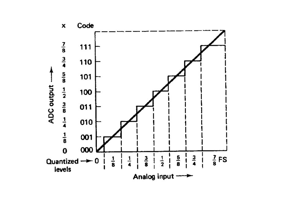
Example2: For a 3 bit ADC which has an input ranging form 0 to 5 V. calculate the following 1. LSB 2. Threshold 3. The range of quantized levels 4. Sketch the relationship between analog input and code Threshold =±0.625mV The range is Form (0 to 0.715) mv
 mv.")
35
Converter Parameter

36
a. Converter Errors a- offset error, b) gain error, c) integral linearity error, d) differential linearity error
 gain error, c) integral linearity error, d) differential linearity error.")
37
Conversion Time Example 3: a 8 bit ADC having a conversion time of 10 S is being used to convert a sinusoidal signal given in the following form Calculate the maximum value of frequency the can be converted by the ADC

38
The maximum rate of change Step1. Calculate the maximum rate of change of analog signal Step2. Calculate FSD of the signal FSD=2A Step3. Apply the following equation f max =12.4Hz Is f=12.4Hz the desired value of conversion ? Answer: this value can be increased using S/H device between input signal and ADC

40
Aperture error We have seen that the conversion of an analog signal to a digital output takes time: the conversion time, which in the case of a successive approximation ADC, is fixed. Now, if the analog input signal is changing during the conversion time, then the converted output will be in error. This is known as aperture error. For example, for an 8-bit ADC, the smallest increment δ of input signal registered by a single bit will be: δ = 1/2 8 = 0.0039 fraction of full scale of signal

41
During conversion time, the signal changes. For there to be no error in the digitised output, this change must be less than the smallest increment registered by a single bit: i.e. the product (δ)(Α).
(Α)..")
42
What does it mean? The ADC08xx series of ICs are 8-bit analog to digital converters which use the successive approximation technique. The conversion time is given by the clock frequency. It takes approximately 64 clock cycles to perform one 8-bit conversion. Thus, to obtain a sampling rate of say 10 000 samples per second, the clock frequency needs to be set to:

43
Sample-and-hold To avoid aperture error, the conversion time and the desired performance characteristics of the ADC circuit must be taken into consideration. For example, given a conversion time of say 100 μsec, what is the maximum frequency of sine wave that can be sampled by the 8-bit ADC0804 without aperture error?

44
We need a circuit that will take a sample of the input voltage at a particular instant, and hold it until the ADC has processed the conversion - a sample and- hold circuit

45
When logic input is high, output follows any changes in the analog input. When logic input goes low, the analog input signal is captured and passed through to the output. Output remains fixed at this value while logic input is held low. The time taken for the sample-and-hold circuit to sample the signal and hold it must be shorter than the conversion time (otherwise we wouldn’t need to use the circuit!). The above circuit has a conversion time of about 10 μsec
. The above circuit has a conversion time of about 10 μsec.")
46
ADC techniques

47
a. Flash analogue-to-digital converter

48
In any n-digit binary ADC there are Q quantisation voltage levels V0 to VQ−1, where Q = 2 n. In a flash ADC there are Q − 1 comparators in parallel and Q − 1 corresponding voltage levels V 1 to V Q−1. There is no need to provide the V0 voltage level. In each comparator q, the input sample value yi is compared with the corresponding voltage level Vq. If yi is less than or equal to Vq, the output is zero corresponding to 0. If yi is greater than Vq, the output is non-zero corresponding to a 1 Operation principle Thus if yi lies between Vq and Vq+1, i.e. Vq < yi ≤ Vq+1, the output of the lowest q comparators 1 to q will all be 1 and the output of the remaining comparators q + 1 to Q − 1 will all be 0. Thus the comparators provide a Q − 1 digit parallel input code to a priority encoder which generates an n-digit binary parallel output code corresponding to the value of q. The main advantage of the flash converter is the short conversion time; the main disadvantage is that the large number of comparators required to give acceptable resolution mean that it is relatively expensive.

49
b. Single-Slope ADC Architecture Single-slope ADC circuit Response of single slope ADC or -de-integrate time -integrate time

50
Operation principle Here, an unknown input voltage is integrated and the value is compared against a known reference value. The time it takes for the integrator to trip the comparator is proportional to the unknown voltage (V INT /V IN ). In this case, the known reference voltage must be stable and accurate to guarantee the accuracy of the measurement. Drawback the accuracy is also dependent on the tolerances of the integrator’s R and C values.
. In this case, the known reference voltage must be stable and accurate to guarantee the accuracy of the measurement. Drawback the accuracy is also dependent on the tolerances of the integrator’s R and C values..")
51
c. Dual-Slope ADC Architecture Dual-slope ADC circuit system

52
Response of dual slope ADC A dual-slope ADC (DS-ADC) integrates an unknown input voltage (V IN ) for a fixed amount of time (T INT ), then “disintegrates” (T DEINT ) using a known reference voltage (V REF ) for a variable amount of time. The key advantage of this architecture over the single-slope is that the final conversion result is insensitive to errors in the component values. That is, any error introduced by a component value during the integrate cycle will be canceled out during the de-integrate phase Operation principle

53
Dual slope – principle

54
D) successive approximation analogue to digital converter
 successive approximation analogue to digital converter")
55
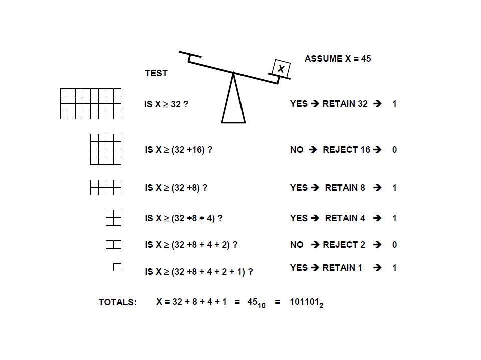
This method involves making successive guesses at the binary code corresponding to the input voltage yi. The trial code is converted into an analogue voltage using a DAC, and a comparator is used to decide whether the guess is too high or too low. On the basis of this result another guess is made, and the process is repeated until Vq is within half a quantisation interval of yi. Operation principle Refer to the table The first guess is always 01111111 corresponding to (127)10, i.e. approximately half full scale: this guess is high so that b7 is set to 0; if the guess had been low b7 would be set to 1. The next guess is 00111111 corresponding to (63)10, i.e. approximately one-quarter full scale; this guess is also high so that b6 is confirmed as 0. The process continues until all the remaining bits have been confirmed; the DATA VALID signal then changes state.
10, i.e. approximately half full scale: this guess is high so that b7 is set to 0; if the guess had been low b7 would be set to 1. The next guess is corresponding to (63)10, i.e. approximately one-quarter full scale; this guess is also high so that b6 is confirmed as 0. The process continues until all the remaining bits have been confirmed; the DATA VALID signal then changes state..")
57
a series of guesses for an 8-bit binary converter with an input range of 0 to 2.55 V

58
Successive approximation converters (SAC) can be used for sample rates up to over 10 6 samples/s; even 16-bit types can be used up to over 10 5 samples/s. For the fastest applications up to 10 9 samples/s, such as video digitisation, flash converters are used. SAC converters can be linked to microcontrollers using two-way serial communication over a pair of wires. Here the successive approximation logic is provided by the microcontroller; the SAC consists only of a DAC and a comparator. The microcontroller sends out clock pulses to operate the DAC switches and receives the digital code in serial form. Application of SAC

59
In this method, the input voltage is compared to half the full scale voltage and then lower values in succession. The steps are:

Similar presentations


>")
 And>")


 Interfacing a microprocessor-based system.>")
 is a device that converts continuous signals to discrete.>")
 Conversion An overview of A/D techniques.>")


>")


