Download presentation
Presentation is loading. Please wait.

1
CoE3DJ4 Digital Systems Design Register transfers, sequencing and control (from chapters 7 and 8 of Mano and Kime)
")
2
Register Transfers A digital system is a sequential circuit made up of interconnected flip-flops and gates We saw that sequential circuits can be specified by means of state tables To specify a large digital system with state table is very difficult, because the number of states is prohibitively large To overcome, digital systems are designed using a modular hierarchical approach

3
Datapath, control System is partitioned into subsystems or modules, each of which performs some task The modules are constructed hierarchically from functional blocks such as registers, counters, decoders, … Subsystems communicate with data and control signals to form a digital system In digital system design, we partition the system into two types of modules: datapath and control –Datapath: perform data processing operations –Control unit: determines the sequence of those operations

4
Datapath, control Control signals: binary signals that activate various data processing operations Control unit receives status bits from the datapath, which describe aspects of the state of the datapath Status bits are used by control unit in defining sequence of operations to be performed

5
Datapath Datapaths are defined by their registers and operations performed on data stored in registers Movement of data stored in registers and processing performed on data are referred to as register transfer operations A register has the capability to perform one or more elementary operations such as load, count, add, subtract and shift An elementary operation performed on data stored in registers is called a microoperation.

6
Datapath Microoperations most often encountered in digital systems: are –transfer –arithmetic –logic –shift

7
Register Transfers

8
Conditional transfer: if(K1=1) then R2 R1 K1: R2 R1
 then R2 R1 K1: R2 R1")
9
Arithmetic Microoperations Multiplication and division are not included because they can be implemented by a sequence of basic microoperations

10
X’K1: R1 R1+R2 XK1: R1 R1+R2’+1 Arithmetic Microoperations

11
Logic Microoperations

12
Shift Microoperations

13
Control unit Binary information in a digital system can be classified as either data or control information Data is manipulated in a datapath by microoperations. These operations are implemented with adder-subtractors, shifters, registers, multiplexers and buses. Control unit provides signals that activate various microoperations in the datapath

14
Control unit Control unit is a sequential circuit with states that dictate control signals for the system At a given time, the state of the sequential circuit activates a prescribed set of microoperations. Using status conditions, control inputs and its current state control unit determines its next state.

15
Control unit Digital systems can be divided into programmable and nonprogrammable depending on the type of control unit Nonprogrammable systems: have inputs, do not have any mechanism for executing programs Programmable systems: can execute programs In a programmable system a portion of the input consists of sequence of instructions. Instruction specifies the operation to be preformed, which operands to use, where to place the results.

16
Control unit For programmable systems, instructions are stored in memory (RAM or ROM). To execute the instructions in sequence, the address of the instruction to be performed is required This address comes from a register called program counter (PC). Executing an instruction means activating the necessary sequence of microoperations in the datapath required to perform the instruction
. Executing an instruction means activating the necessary sequence of microoperations in the datapath required to perform the instruction.")
17
Control unit For a nonprogrammable system, the control unit is not responsible for obtaining instruction from memory, nor it is responsible for sequencing the execution of those instructions. There is no PC in such a system We focus on nonprogrammable systems using multiplier for illustration We use algorithmic state machines (ASMs) for control unit design.
 for control unit design..")
18
Algorithmic state machines A processing task can be defined by register transfer microoperations controlled by a sequencing mechanism This task can be specified as a hardware algorithm A flowchart is a convenient way to specify a sequence of procedural steps and decision paths for an algorithm We use a special flowchart called an algorithmic state machine (ASM) chart to define digital hardware algorithms ASM chart resembles a conventional flowchart, but is interpreted differently ASM provides not only a sequence of events, but the timing relationship between states of control unit and datapath actions
 chart to define digital hardware algorithms ASM chart resembles a conventional flowchart, but is interpreted differently ASM provides not only a sequence of events, but the timing relationship between states of control unit and datapath actions")
19
Algorithmic state machines ASM chart contains three basic elements: state box, scalar decision box, and the conditional output box. For convenience a fourth element, vector decision box is added.

20
Algorithmic state machines A state in control sequence is indicated by a state box. State box contains register transfer operations or output signals that are activated while the control unit is in the state. Symbolic name of the state is placed at the upper left corner of the box and the binary code (if assigned) is placed at the upper right corner of the box Decision box describes the effects of an input or status signals on the control The condition is a single binary input variable or a Boolean expression
 is placed at the upper right corner of the box Decision box describes the effects of an input or status signals on the control The condition is a single binary input variable or a Boolean expression.")
21
Algorithmic state machines Entry path to a conditional output box is from a decision box Vector decision box describes the effects of a vector input on the control For an n-element input vector, 2 n exit paths exist depending on the value of the input

22
Algorithmic state machines

23
Relation between ASM chart and state diagram of control unit: Each state box is equivalent to a node in the state diagram Decision boxes are equivalent to input values on lines connecting nodes in diagram Register transfers and outputs in state boxes would be specified on a state node in state diagram (Moore dependency) Register transfers and outputs in conditional output boxes correspond to outputs on lines connecting nodes in state diagram (Mealy dependency)
 Register transfers and outputs in conditional output boxes correspond to outputs on lines connecting nodes in state diagram (Mealy dependency)")
24
Algorithmic state machines

25
Figure 10.15 An algorithm for multiplication (a)Manualmethod P=0 ; for i=0 to n1 do if b i =1 then P=P+A ; endif; Left-shift A ; endfor; (b)Pseudo-code Multiplicand1 1 Product Multiplier1 0 0 1 1 1 1 1 0 1 1011 0000 1011 010 0 1 1 1 1 Binary 13 11 13 143 Decimal – ASM example (binary multiplier)
Manualmethod P=0 ; for i=0 to n1 do if b i =1 then P=P+A ; endif; Left-shift A ; endfor; (b)Pseudo-code Multiplicand1 1 Product Multiplier Binary Decimal – ASM example (binary multiplier)")
26
Figure 10.16 ASM chart for the multiplier Shift left A,Shift rightBDone PPA+ B0=? P0 s Load A b 0 Reset S3 0 1 0 1 0 1 s S1 S2 1 0 Load B

27
Figure 10.17 Datapath circuit for the multiplier E L E L E 0DataALA EA A Clock P DataP Register EP Sum 0 z B b 0 DataBLB EB + 2n n n Shift-left register Shift-right register n n 2n Psel 10 2n

28
Figure 10.18 ASM chart for the multiplier control circuit EP z b 0 Reset S3 0 1 0 1 s 0 1 Done Psel0=EP s 0 1 S1 S2 LA EA LB EB 0 1 0 1 Psel1=EAEB

29
Figure 10.19a VHDL code for the multiplier circuit LIBRARY ieee ; USE ieee.std_logic_1164.all ; USE ieee.std_logic_unsigned.all ; USE work.components.all ; ENTITY multiply IS GENERIC ( N : INTEGER := 8; NN : INTEGER := 16 ) ; PORT (Clock : IN STD_LOGIC ; Resetn : IN STD_LOGIC ; LA, LB, s : IN STD_LOGIC ; DataA : IN STD_LOGIC_VECTOR(N-1 DOWNTO 0) ; DataB : IN STD_LOGIC_VECTOR(N-1 DOWNTO 0) ; P : BUFFER STD_LOGIC_VECTOR(NN-1 DOWNTO 0) ; Done : OUT STD_LOGIC ) ; END multiply ; ARCHITECTURE Behavior OF multiply IS TYPE State_type IS ( S1, S2, S3 ) ; SIGNAL y : State_type ; SIGNAL Psel, z, EA, EB, EP, Zero : STD_LOGIC ; SIGNAL B, N_Zeros : STD_LOGIC_VECTOR(N-1 DOWNTO 0) ; SIGNAL A, Ain, DataP, Sum : STD_LOGIC_VECTOR(NN-1 DOWNTO 0) ; BEGIN … con’t
 ; PORT (Clock : IN STD_LOGIC ; Resetn : IN STD_LOGIC ; LA, LB, s : IN STD_LOGIC ; DataA : IN STD_LOGIC_VECTOR(N-1 DOWNTO 0) ; DataB : IN STD_LOGIC_VECTOR(N-1 DOWNTO 0) ; P : BUFFER STD_LOGIC_VECTOR(NN-1 DOWNTO 0) ; Done : OUT STD_LOGIC ) ; END multiply ; ARCHITECTURE Behavior OF multiply IS TYPE State_type IS ( S1, S2, S3 ) ; SIGNAL y : State_type ; SIGNAL Psel, z, EA, EB, EP, Zero : STD_LOGIC ; SIGNAL B, N_Zeros : STD_LOGIC_VECTOR(N-1 DOWNTO 0) ; SIGNAL A, Ain, DataP, Sum : STD_LOGIC_VECTOR(NN-1 DOWNTO 0) ; BEGIN … con’t")
30
Figure 10.19b VHDL code for the multiplier circuit (con’t) FSM_transitions: PROCESS ( Resetn, Clock ) BEGIN IF Resetn = '0' THEN y <= S1 ; ELSIF (Clock'EVENT AND Clock = '1') THEN CASE y IS WHEN S1 => IF s = '0' THEN y <= S1 ; ELSE y <= S2 ; END IF ; WHEN S2 => IF z = '0' THEN y <= S2 ; ELSE y <= S3 ; END IF ; WHEN S3 => IF s = '1' THEN y <= S3 ; ELSE y <= S1 ; END IF ; END CASE ; END IF ; END PROCESS ; FSM_outputs: PROCESS ( y, s, LA, LB, B(0) ) BEGIN EP <= '0' ; EA <= '0' ; EB <= '0' ; Done <= '0' ; Psel <= '0'; CASE y IS WHEN S1 => EP <= '1' ; IF s = '0' AND LA = '1' THEN EA <= '1' ; ELSE EA <= '0' ; END IF ; IF s = '0' AND LB = '1' THEN EB <= '1' ; … con’t
 FSM_transitions: PROCESS ( Resetn, Clock ) BEGIN IF Resetn = 0 THEN y <= S1 ; ELSIF (Clock EVENT AND Clock = 1 ) THEN CASE y IS WHEN S1 => IF s = 0 THEN y <= S1 ; ELSE y <= S2 ; END IF ; WHEN S2 => IF z = 0 THEN y <= S2 ; ELSE y <= S3 ; END IF ; WHEN S3 => IF s = 1 THEN y <= S3 ; ELSE y <= S1 ; END IF ; END CASE ; END IF ; END PROCESS ; FSM_outputs: PROCESS ( y, s, LA, LB, B(0) ) BEGIN EP <= 0 ; EA <= 0 ; EB <= 0 ; Done <= 0 ; Psel <= 0 ; CASE y IS WHEN S1 => EP <= 1 ; IF s = 0 AND LA = 1 THEN EA <= 1 ; ELSE EA <= 0 ; END IF ; IF s = 0 AND LB = 1 THEN EB <= 1 ; … con’t")
31
Figure 10.19c VHDL code for the multiplier circuit (con’t) ELSE EB <= '0' ; END IF ; WHEN S2 => EA <= '1' ; EB <= '1' ; Psel <= '1' ; IF B(0) = '1' THEN EP <= '1' ; ELSE EP <= '0' ; END IF ; WHEN S3 => Done <= '1' ; END CASE ; END PROCESS ; -- Define the datapath circuit Zero '0' ) ; Ain <= N_Zeros & DataA ; ShiftA: shiftlne GENERIC MAP ( N => NN ) PORT MAP ( Ain, LA, EA, Zero, Clock, A ) ; ShiftB: shiftrne GENERIC MAP ( N => N ) PORT MAP ( DataB, LB, EB, Zero, Clock, B ) ; z <= '1' WHEN B = N_Zeros ELSE '0' ; Sum <= A + P ; -- Define the 2n 2-to-1 multiplexers for DataP GenMUX: FOR i IN 0 TO NN-1 GENERATE Muxi: mux2to1 PORT MAP ( Zero, Sum(i), Psel, DataP(i) ) ; END GENERATE; RegP: regne GENERIC MAP ( N => NN ) PORT MAP ( DataP, Resetn, EP, Clock, P ) ; END Behavior ;
 ELSE EB <= 0 ; END IF ; WHEN S2 => EA <= 1 ; EB <= 1 ; Psel <= 1 ; IF B(0) = 1 THEN EP <= 1 ; ELSE EP <= 0 ; END IF ; WHEN S3 => Done <= 1 ; END CASE ; END PROCESS ; -- Define the datapath circuit Zero 0 ) ; Ain <= N_Zeros & DataA ; ShiftA: shiftlne GENERIC MAP ( N => NN ) PORT MAP ( Ain, LA, EA, Zero, Clock, A ) ; ShiftB: shiftrne GENERIC MAP ( N => N ) PORT MAP ( DataB, LB, EB, Zero, Clock, B ) ; z <= 1 WHEN B = N_Zeros ELSE 0 ; Sum <= A + P ; -- Define the 2n 2-to-1 multiplexers for DataP GenMUX: FOR i IN 0 TO NN-1 GENERATE Muxi: mux2to1 PORT MAP ( Zero, Sum(i), Psel, DataP(i) ) ; END GENERATE; RegP: regne GENERIC MAP ( N => NN ) PORT MAP ( DataP, Resetn, EP, Clock, P ) ; END Behavior ;")
32
Figure 10.3 VHDL code for an n-bit register with an enable input LIBRARY ieee ; USE ieee.std_logic_1164.all ; ENTITY regne IS GENERIC ( N : INTEGER := 4 ) ; PORT (R : IN STD_LOGIC_VECTOR(N-1 DOWNTO 0) ; Resetn: IN STD_LOGIC ; E, Clock: IN STD_LOGIC ; Q : OUT STD_LOGIC_VECTOR(N-1 DOWNTO 0) ) ; END regne ; ARCHITECTURE Behavior OF regne IS BEGIN PROCESS ( Resetn, Clock ) BEGIN IF Resetn = '0' THEN Q '0') ; ELSIF Clock'EVENT AND Clock = '1' THEN IF E = '1' THEN Q <= R ; END IF ; END PROCESS ; END Behavior ;
 ; PORT (R : IN STD_LOGIC_VECTOR(N-1 DOWNTO 0) ; Resetn: IN STD_LOGIC ; E, Clock: IN STD_LOGIC ; Q : OUT STD_LOGIC_VECTOR(N-1 DOWNTO 0) ) ; END regne ; ARCHITECTURE Behavior OF regne IS BEGIN PROCESS ( Resetn, Clock ) BEGIN IF Resetn = 0 THEN Q 0 ) ; ELSIF Clock EVENT AND Clock = 1 THEN IF E = 1 THEN Q <= R ; END IF ; END PROCESS ; END Behavior ;")
33
Figure 10.4a Code for a right-to-left shift register with an enable input LIBRARY ieee ; USE ieee.std_logic_1164.all ; -- right-to-left shift register with parallel load and enable ENTITY shiftlne IS GENERIC ( N : INTEGER := 4 ) ; PORT(R : IN STD_LOGIC_VECTOR(N-1 DOWNTO 0) ; L, E, w : IN STD_LOGIC ; Clock : IN STD_LOGIC ; Q : BUFFER STD_LOGIC_VECTOR(N-1 DOWNTO 0) ) ; END shiftlne ; ARCHITECTURE Behavior OF shiftlne IS BEGIN PROCESS BEGIN … con’t
 ; PORT(R : IN STD_LOGIC_VECTOR(N-1 DOWNTO 0) ; L, E, w : IN STD_LOGIC ; Clock : IN STD_LOGIC ; Q : BUFFER STD_LOGIC_VECTOR(N-1 DOWNTO 0) ) ; END shiftlne ; ARCHITECTURE Behavior OF shiftlne IS BEGIN PROCESS BEGIN … con’t")
34
Figure 10.4b Code for a right-to-left shift register with an enable input (con’t) … con’t WAIT UNTIL Clock'EVENT AND Clock = '1' ; IF E = '1' THEN IF L = '1' THEN Q <= R ; ELSE Q(0) <= w ; Genbits: FOR i IN 1 TO N-1 LOOP Q(i) <= Q(i-1) ; END LOOP ; END IF ; END PROCESS ; END Behavior ;
 … con’t WAIT UNTIL Clock EVENT AND Clock = 1 ; IF E = 1 THEN IF L = 1 THEN Q <= R ; ELSE Q(0) <= w ; Genbits: FOR i IN 1 TO N-1 LOOP Q(i) <= Q(i-1) ; END LOOP ; END IF ; END PROCESS ; END Behavior ;")
35
Figure 6.27 VHDL code for a 2-to-1 multiplexer LIBRARY ieee ; USE ieee.std_logic_1164.all ; ENTITY mux2to1 IS PORT (w0, w1, s: IN STD_LOGIC ; f: OUT STD_LOGIC ) ; END mux2to1 ; ARCHITECTURE Behavior OF mux2to1 IS BEGIN WITH s SELECT f <=w0 WHEN '0', w1 WHEN OTHERS ; END Behavior ;
 ; END mux2to1 ; ARCHITECTURE Behavior OF mux2to1 IS BEGIN WITH s SELECT f <=w0 WHEN 0 , w1 WHEN OTHERS ; END Behavior ;")
36
Figure 10.5a Component declaration statements for building blocks LIBRARY ieee ; USE ieee.std_logic_1164.all ; PACKAGE components IS -- 2-to-1 multiplexer COMPONENT mux2to1 PORT (w0, w1 : IN STD_LOGIC ; s : IN STD_LOGIC ; f : OUT STD_LOGIC ) ; END COMPONENT ; -- D flip-flop with 2-to-1 multiplexer connected to D COMPONENT muxdff PORT (D0, D1, Sel, Clock : IN STD_LOGIC ; Q : OUT STD_LOGIC ) ; END COMPONENT ; -- n-bit register with enable COMPONENT regne GENERIC ( N : INTEGER := 4 ) ; PORT (R : IN STD_LOGIC_VECTOR(N-1 DOWNTO 0) ; Resetn : IN STD_LOGIC ; E, Clock : IN STD_LOGIC ; Q : OUT STD_LOGIC_VECTOR(N-1 DOWNTO 0) ) ; END COMPONENT ; … con’t
 ; END COMPONENT ; -- D flip-flop with 2-to-1 multiplexer connected to D COMPONENT muxdff PORT (D0, D1, Sel, Clock : IN STD_LOGIC ; Q : OUT STD_LOGIC ) ; END COMPONENT ; -- n-bit register with enable COMPONENT regne GENERIC ( N : INTEGER := 4 ) ; PORT (R : IN STD_LOGIC_VECTOR(N-1 DOWNTO 0) ; Resetn : IN STD_LOGIC ; E, Clock : IN STD_LOGIC ; Q : OUT STD_LOGIC_VECTOR(N-1 DOWNTO 0) ) ; END COMPONENT ; … con’t")
37
Figure 10.5b Component declaration statements for building blocks (con’t) … con’t -- n-bit right-to-left shift register with parallel load and enable COMPONENT shiftlne GENERIC ( N : INTEGER := 4 ) ; PORT (R : IN STD_LOGIC_VECTOR(N-1 DOWNTO 0) ; L, E, w: IN STD_LOGIC ; Clock: IN STD_LOGIC ; Q : BUFFER STD_LOGIC_VECTOR(N-1 DOWNTO 0) ) ; END COMPONENT ; -- n-bit left-to-right shift register with parallel load and enable COMPONENT shiftrne GENERIC ( N : INTEGER := 4 ) ; PORT (R : IN STD_LOGIC_VECTOR(N-1 DOWNTO 0) ; L, E, w: IN STD_LOGIC ; Clock: IN STD_LOGIC ; Q : BUFFER STD_LOGIC_VECTOR(N-1 DOWNTO 0) ) ; END COMPONENT ; … con’t
 … con’t -- n-bit right-to-left shift register with parallel load and enable COMPONENT shiftlne GENERIC ( N : INTEGER := 4 ) ; PORT (R : IN STD_LOGIC_VECTOR(N-1 DOWNTO 0) ; L, E, w: IN STD_LOGIC ; Clock: IN STD_LOGIC ; Q : BUFFER STD_LOGIC_VECTOR(N-1 DOWNTO 0) ) ; END COMPONENT ; -- n-bit left-to-right shift register with parallel load and enable COMPONENT shiftrne GENERIC ( N : INTEGER := 4 ) ; PORT (R : IN STD_LOGIC_VECTOR(N-1 DOWNTO 0) ; L, E, w: IN STD_LOGIC ; Clock: IN STD_LOGIC ; Q : BUFFER STD_LOGIC_VECTOR(N-1 DOWNTO 0) ) ; END COMPONENT ; … con’t")
38
Figure 10.5c Component declaration statements for building blocks (con’t) … con’t -- up-counter that counts from 0 to modulus-1 COMPONENT upcount GENERIC( modulus : INTEGER := 8 ) ; PORT( Resetn : IN STD_LOGIC ; Clock, E, L: IN STD_LOGIC ; R : IN INTEGER RANGE 0 TO modulus-1 ; Q : BUFFER INTEGER RANGE 0 TO modulus-1 ) ; END COMPONENT ; -- down-counter that counts from modulus-1 down to 0 COMPONENT downcnt GENERIC( modulus : INTEGER := 8 ) ; PORT (Clock, E, L: IN STD_LOGIC ; Q : BUFFER INTEGER RANGE 0 TO modulus-1 ) ; END COMPONENT ; END components ;
 … con’t -- up-counter that counts from 0 to modulus-1 COMPONENT upcount GENERIC( modulus : INTEGER := 8 ) ; PORT( Resetn : IN STD_LOGIC ; Clock, E, L: IN STD_LOGIC ; R : IN INTEGER RANGE 0 TO modulus-1 ; Q : BUFFER INTEGER RANGE 0 TO modulus-1 ) ; END COMPONENT ; -- down-counter that counts from modulus-1 down to 0 COMPONENT downcnt GENERIC( modulus : INTEGER := 8 ) ; PORT (Clock, E, L: IN STD_LOGIC ; Q : BUFFER INTEGER RANGE 0 TO modulus-1 ) ; END COMPONENT ; END components ;")
39
ASM example (binary multiplier)
")
40
Counter P requires bits C is a flip-flop that can be either synchronously cleared to 0 or loaded from Cout. Multiplicand is loaded into register B from IN. Multiplier is loaded into register Q from IN Partial product is formed in register A and stored in registers A and Q. C flip-flop stores carry Cout, whether 0 or 1 and is reset to 0 during the right shift P is initially set to n-1 and counted down after the formation of each partial product

41
ASM example (binary multiplier)
")
42
Value of P is checked before it is decremented n operations occur, one operation for each value in P, n-1 down to 0 When P is 0, final product is in double registers A and Q. Control unit stays in an initial state until Go signal G becomes 1, then the system starts multiplication Sum of A and B forms n most significant bits of the partial product which is transferred back to A. Cout is transferred to C Both partial product in A and the multiplier in Q are shifted to the right

43
ASM example (binary multiplier) Carry from C shifts into most significant bit of A, least significant bit of A shifts into the most significant bit of Q and the least significant bit of Q is discarded. Least significant bit of Q, Q0 always holds the nit of the multiplier that the control unit examines text Control unit decides whether to add based on the value of this bit Control unit checks signal Z, which is 1 for P equal to zero to determine whether the multiplication is finished Q0 and Z are status inputs for control unit and G is external control input

44
ASM example (binary multiplier)
")
45
In implementing a control unit, two distinct aspects must be considered: 1) part of the control unit that generates the control signals 2) part of the control that determines what happens next We separate these two aspects by dividing the original ASM specifications into two parts: a table that defines control signals in terms of states and inputs and a simplified ASM chart that represents only transitions from state to state
 part of the control unit that generates the control signals 2) part of the control that determines what happens next We separate these two aspects by dividing the original ASM specifications into two parts: a table that defines control signals in terms of states and inputs and a simplified ASM chart that represents only transitions from state to state")
46
ASM example (binary multiplier) One approach to determine the control signals needed is to examine datapath registers and tabulated the microoperations for each register. Based on the microoperations, control signals are defined. A control signal can be used for activating microoperations in more than one register The Boolean expression for each control signal is derived from the location or locations of the microoperation in the ASM chart.

47
ASM example (binary multiplier) Since clear operation of A always occurs at the same time as loading of P, both microoperations can be activated by the same control signal named Initialize. The Boolean expression for Initialize is determined from the ASM chart.

48
ASM example (binary multiplier) After taking care of control signals, we can redraw the ASM chart so that only information on sequencing is represented. We remove all the conditional output boxes. Also any decision box not affecting the next state is removed. The modified ASM chart can be treated as a state diagram and a sequential circuit can be designed for it using a state table In many cases this is difficult to carry out because of large number of states for a typical control unit We use specialized methods for control unit design: 1) sequence register and decoder 2) one flip-flop per state
 sequence register and decoder 2) one flip-flop per state.")
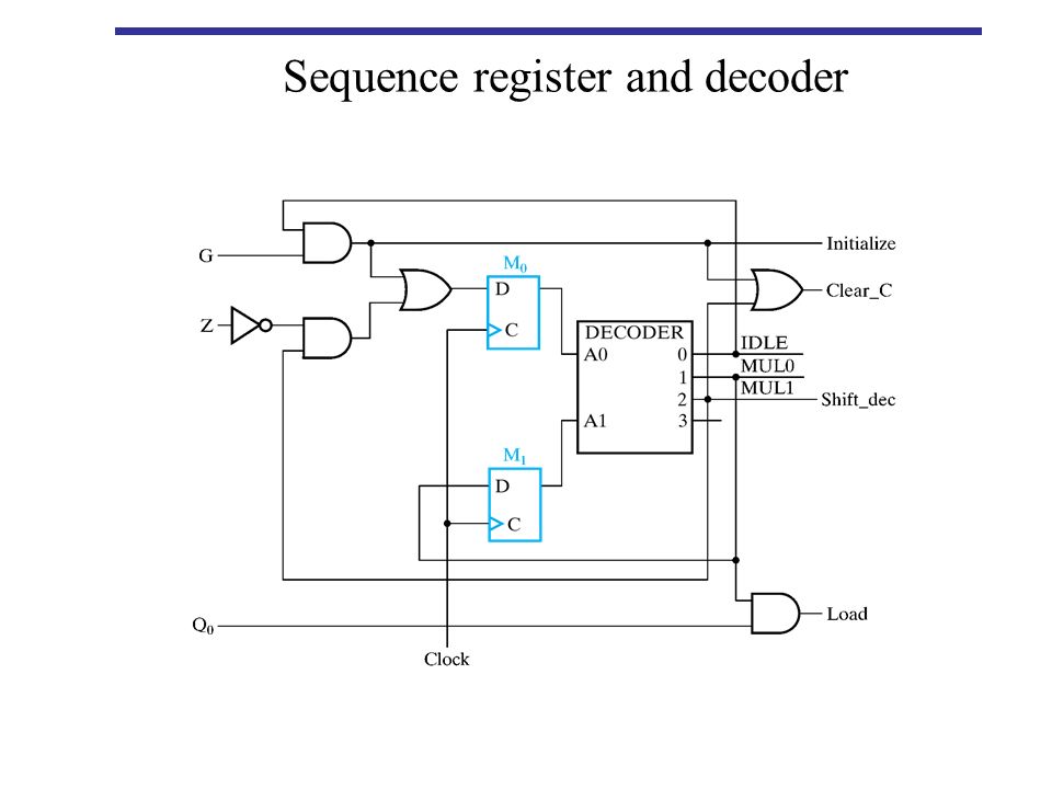
49
Sequence register and decoder Uses a sequence register for the state and a decoder to provide an output corresponding to each of the states. A register with n flip-flops can have up to 2 n states and an n- to-2 n decoder has up to 2 n outputs one for each of the states. Additional logic may be required to produce the necessary output (control) signals. Combinational circuit Flip-flops Clock W Z Combinational circuit sequence register Decoder
 signals. Combinational circuit Flip-flops Clock W Z Combinational circuit sequence register Decoder.")
50
Sequence register and decoder Sequencing part of ASM chart of the binary multiplier has three states and two inputs. To implement the ASM chart with a sequence register and decoder, we need two flip-flops for register and a 2-to-4-line decoder Since there are three states only three of four outputs of the decoder are used.

51
Sequence register and decoder The state table is given in the next slide. Binary states 00, 01 and 10 are assigned to IDEL, MUL0 and MUL1. The input columns have unspecified entries whenever an input variable is not used to determine the next state. The binary code for the present state determines the particular decoder output that is equal to one. –Present state M 1 M 0 =00 output IDLE =1 Since the states are available (outputs of decoder), the input combinational logic for each flip-flop can be easily obtained by inspection of the table D M0 =IDLE.G+MUL1.Z’ D M1 =MUL0
, the input combinational logic for each flip-flop can be easily obtained by inspection of the table D M0 =IDLE.G+MUL1.Z’ D M1 =MUL0.")
52
Sequence register and decoder

54
One flip-flop per state A flip-flop is assigned to each of the states and at any time only one of the flip-flops contains a 1. The single 1 propagates from one flip-flop to another under the control of decision logic Although this method uses the maximum number of flip- flops, it simplifies the logic design A modified ASM chart can be transformed into a sequential circuit with one flip-flop per state by symbol replacement rules

55
One flip-flop per state

57
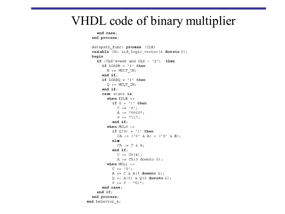
VHDL code of binary multiplier

Similar presentations

 part 1. ASM2 Algorithmic State Machine (ASM) Our design methodologies do not scale well to real-world problems.>")


 Terms of Use Chapter 7 – Registers.>")


>")


 Charts,>")
 School of Computing, UNF.>")


