Download presentation
Presentation is loading. Please wait.

1
CCTC MFG Capabilities & Technology Roadmap 2010

2
CCTC Manufacturing Capabilities
SIZE Maximum Processed finish board size 22 X 16inch Average Processed finish board size 8 X 6inch Board Size Tolerance ±0.004inch Maximum Panel Size 24 X 24inch Minimum Panel Size 14 X 10inch THICKNESS Maximum Processed Thickness .250inch Average Processed Thickness .062inch Board Thickness Tolerance +/-10% Warp / Bow and Twist - Inch per Inch ≤0.5% LAYER CONSTRUCTION Maximum Processed Layer Count 28 Average Processed Layer Count 8 Minimum Dielectric Thickness (not including Microvia layers) .002inch Minimum Core Thickness 0.004inch Layer to Layer Registration .003inch Dielectric Tolerance Layer to Layer ±10%
 .002inch. Minimum Core Thickness inch. Layer to Layer Registration. .003inch. Dielectric Tolerance Layer to Layer. ±10%")
3
Minimum Mechanically Drilled Hole size Preferred
CCTC Manufacturing Capabilities ASPECT RATIO Maximum Aspect Ratio - Plated Through Holes 10: 1 Maximum Aspect Ratio - Microvia Holes 1: 1 Minimum Drill Size - Mechanically Drilled holes prior to plating .008inch Minimum Mechanically Drilled Hole size Preferred .010inch Smallest Finished PTH .006inch Smallest Finished PTH - Tolerance ±.002inch Nominal Finished PTH .023inch Nominal Finished PTH - Tolerance ±.003inch HOLE SIZE TOLERANCE PTH Standard PTH Compliant Pin NPTH True Position Tolerance

4
CONDUCTOR WIDTH Minimum Inner Layer Width .003inch Typical Inner Layer Width .005inch Minimum Outer Layer Width Typical Outer Layer Width Minimum Trace on 3 oz base copper +/-.002 Minimum Trace on 4 oz base copper Minimum Trace on 5 oz base copper +/-.003 CONDUCTOR SPACE Minimum Inner Layer Space - Trace to Trace Typical Inner Layer Space - Trace to trace Minimum Outer Layer Space - Trace to Trace Typical Outer Layer Space - Trace to trace Minimum SMD Land Pattern Pitch 0.016inch CONTROLLED IMPEDANCE Impedance Typical - Value Ohms 50 , 75 , 100 Impedance Typical - Tolerance ±10% Maximum Impedance Capability - Value Ohms 150 Minimum Impedance Capability - Value Ohms 28 Maximum Impedance Capability - Tolerance ±20%(value < 50 Ohms) Minimum Impedance Capability - Tolerance ±8%(single ended impedance value > 100 Ohms) Impedance Modeling Tool (Type/Name) (I.e.True FieldSolver) Polar CITS25 Impedance Measurement Technique (Equipment/Type) Polar CITS500S Differential Impedance Measurement Technique (Equipment/Type)
 Minimum Impedance Capability - Tolerance. ±8%(single ended impedance value > 100 Ohms) Impedance Modeling Tool (Type/Name) (I.e.True FieldSolver) Polar CITS25. Impedance Measurement Technique (Equipment/Type) Polar CITS500S. Differential Impedance Measurement Technique (Equipment/Type)")
5
CCTC Heavy Copper Capability
Item Normal cap. Special Cap. Layer ≤8 5oz min. line/space Inner layer 16/16 mil 14/14 mil Outer layer (finish) 12/12 mil 10/10 mil 3oz min. line/space 8/8 mil 7/7 mil Line tolerance Inner 3OZ ±2 mil ±1.5 mil Inner 5OZ ±3 mil ±2.5 mil Min. Drill bit mm 20 mil 16 mil
 12/12 mil. 10/10 mil. 3oz min. line/space. 8/8 mil. 7/7 mil. Line tolerance. Inner 3OZ. ±2 mil. ±1.5 mil. Inner 5OZ. ±3 mil. ±2.5 mil. Min. Drill bit. mm. 20 mil. 16 mil.")
6
CCTC Heavy Copper Capability
Item Normal Cap. Special Cap. Min. copper clearance 3OZ ≥12mil 5OZ ≥15mil Inner layer annular ring (to drill bit) Inner 3OZ ≥9 mil ≥8mil Inner 5OZ ≥15 mil Dielectric Thickness Inner 3OZ、Copper density≥70% ≥0.15mm Inner 3OZ、35%≤copper density<70% 0.25mm ≥0.2mm
 Inner 3OZ. ≥9 mil. ≥8mil. Inner 5OZ. ≥15 mil. Dielectric Thickness. Inner 3OZ、Copper density≥70% ≥0.15mm. Inner 3OZ、35%≤copper density<70% 0.25mm. ≥0.2mm.")
7
CCTC Heavy Copper Capability
Item Normal capability Special capability Hole to Line mil ≥9mil ≥8mil Min. Legend width ≥5.5 5.0≤X<5.5 Min. Legend space ≥7.5 6≤X<7.5 Inner layer copper density Inner 3OZ ≥35% Inner 5OZ ≥80%

8
CCTC HDI Manufacturing Capabilities
TECHNOLOGY Buried Vias - Conventional YES Blind Vias - Conventional Blind Micro vias - How many sequential layers of Micro vias (one side) 3 Buried Micro vias (through an individual internal laminate) Buried Resistors - Omega N/A Buried Resistors – Printed Buried Capacitance Conductive Via Fill (CB100) Other Specify Flex (Layer Count) Rigid Flex
 3. Buried Micro vias (through an individual internal laminate) Buried Resistors - Omega. N/A. Buried Resistors – Printed. Buried Capacitance. Conductive Via Fill (CB100) Other Specify. Flex (Layer Count) Rigid Flex.")
9
CCTC Manufacturing Capabilities
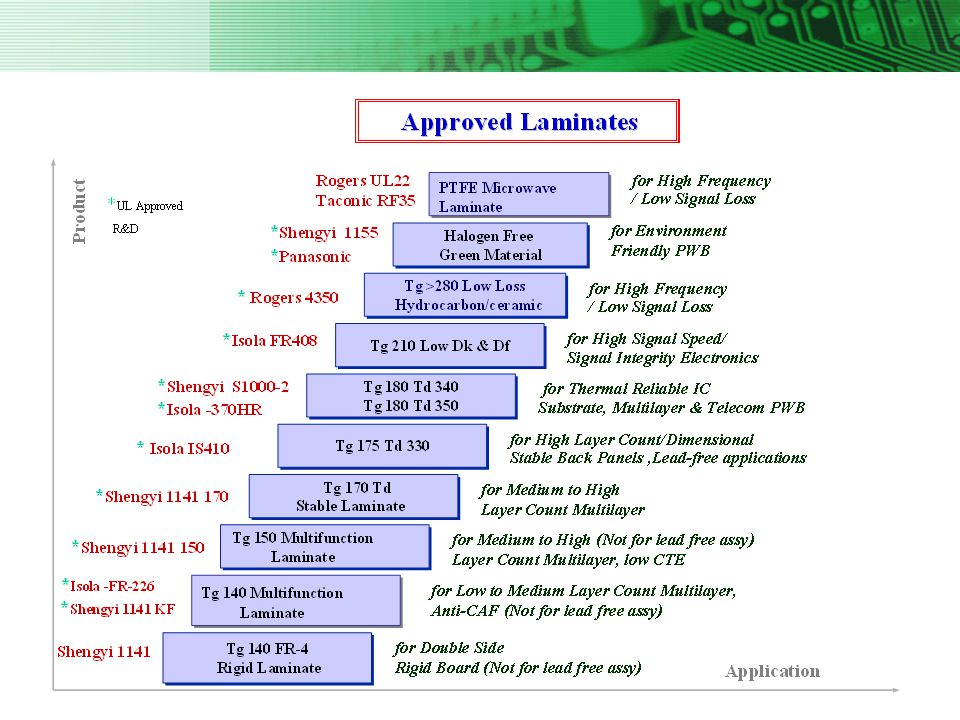
LAMINATE MATERIALS Supplier FR4 Standard Di-Functional Tg = Shengyi S1000-2, Isola HR370 FR4 Standard Multifunctional Tg = 170℃ Iteq , GW , Grace FR4 Tetra functional Tg = 140℃ Shengyi , GW , Grace Resin Coated Copper Tg = 140℃ LG Chemical Getek-Nelco-13 N/A Getek-Nelco-13 Equivalent Isola FR408HR Polyimide Arlon , Isola BT Epoxy Isola, MGC Cyanate Ester PTFE - Teflon Arlon Halogen Free Panasonic, Shengyi Rogers RO4350 Rogers Omega-Ply Mixed Dielectrics (specify) Rogers 4350/FR4 Metal Backed Substrates Metal Core
 Rogers 4350/FR4. Metal Backed Substrates. Metal Core.")
11
Basic Property Comparison for Various Material
According to our experiments on lead free material, the experience during the PCB manufacturing and also the feedback from our customers during their assembly, we compared the general property parameters of various lead free material. Please refer to below table: Laminate Type LF HF Tg (℃) /DSC Td-5% (℃)/ TGA IPC-4101B Z-CTE/TMA T-260 (min)/TMA T-288 (min)/ TMA Dk/ 1MHz Df/ Fill Anti CAF Res sys a1/a2 ppm /℃) 50-260℃ Isola PCLFR-370-HR Y N 180 350 IPC-4101B/126 45/220 2.6% 60 20 4.8 0.015 PN FR408 185 IPC-4101B/99 19/230 3.3% 3.6 0.012 MF Shengyi S1000 150 335 48/250 10 4.7 0.011 S1000-2 340 2.8% 0.013 ITEQ IT158TC 40/250 0.016 IT180ATC 45/240 0.017
 /DSC. Td-5% (℃)/ TGA. IPC-4101B. Z-CTE/TMA. T-260 (min)/TMA. T-288 (min)/ TMA. Dk/ 1MHz. Df/ Fill. Anti. CAF. Res sys. a1/a2 ppm /℃) ℃ Isola. PCLFR-370-HR. Y. N IPC-4101B/ / % PN. FR IPC-4101B/99. 19/ % MF. Shengyi. S / S % ITEQ. IT158TC. 40/ IT180ATC. 45/")
12
ELECTRICAL TEST Net List Extraction YES Net List Comparison Simultaneous Top and Bottom 100% Net List Maximum number of Nodes 20000 Other (Specify) PRODUCTION CYCLE TIME Average Production Cycle Time - Days Quick Turn Capability - Days days Average Production Lot Size (Panels) 100 Maximum Production Lot Size (Panels) 300 Minimum Production Lot Size (Panels) 80 IPC Class 2 and 3 YES BELLCORE COMPLIANCE SEC Testing in House SEC Testing Subcontractor N/A SIR Testing in House SIR Testing Subcontractor Solderability Testing (Frequency) Per lot for shipment Steam Age Testing Capability in House Steam Age Testing Subcontractor Gold Porosity Measurement Technique YES ,POROSITY TESTER Gold Roughness Measurement Technique Gold Thickness Measurement Technique X-Ray
 PRODUCTION CYCLE TIME. Average Production Cycle Time - Days. Quick Turn Capability - Days days. Average Production Lot Size (Panels) 100. Maximum Production Lot Size (Panels) 300. Minimum Production Lot Size (Panels) 80. IPC Class 2 and 3. YES BELLCORE COMPLIANCE. SEC Testing in House. SEC Testing Subcontractor. N/A. SIR Testing in House. SIR Testing Subcontractor. Solderability Testing (Frequency) Per lot for shipment. Steam Age Testing Capability in House. Steam Age Testing Subcontractor. Gold Porosity Measurement Technique. YES ,POROSITY TESTER. Gold Roughness Measurement Technique. Gold Thickness Measurement Technique. X-Ray.")
13
CCTC Tech Roadmap Item Current 2011 2012 Mass Production R&D
Resin System FR-4 Tg 180C° Yes --- Halogen Free FR-4 Tg 170C° PTFE Rogers Tg 280C° Limited BT Tg 200 C° Polyimide Tg 260C° RCC and LDP Normal Epoxy Tg 140C° Td 310C° Halogen Free Epoxy Tg 150C°Td 350C° LDP 170C° Current Supplier 1. Shengyi; 2. Grace; 3. Isola; 4. Rogers; 5. MEM; 6. Nanya; 7. Arlon; 8. MGC; 9. Hitachi. 10. Panasonic

14
CCTC Tech Roadmap Item Current 2011 2012 Mass Production R&D
Max. layer count 28 32 40 36 HDI N+C+N 3 4 via on buried hole/ stack via Yes --- Max. Panel size 24” x 20” 28” x 22” 30” x 24” Max. board thickness ( mm / mil ) 5.6 / 220 6.35 / 250 7.0/.276 6.35/250 Min. board thickness 0.4/16 Tolerance of thickness T < 1.0 mm ± 8% ± 7% 1.0 mm ≤ T < 2.0 mm ± 6% T ≥ 2.0 mm ± 10%
 5.6 / / / /250. Min. board thickness. 0.4/16. Tolerance of. thickness. T < 1.0 mm. ± 8% ± 7% 1.0 mm ≤ T < 2.0 mm. ± 6% T ≥ 2.0 mm. ± 10%")
15
CCTC Tech Roadmap Item Current 2011 2012 Mass Production R&D
Min. core thickness ( mm / mil ) 0.1 / 4 0.075 /3 0.075 / 3 0.05 /2 Min. Prepreg thickness ( um / mil ) 50 / 2 --- Min. inner layer base copper thickness ( OZ )/Thick 0.33/ mil --- 0.33/ mil Max. inner layer base copper thickness ( OZ )/Thick 4.0/Ltd mil 5.0/ 7.0mil 3.0/ 3.6 mil Min. outer layer base copper thickness ( OZ )/Thick 0.33/ mil Max. outer layer base copper thickness ( OZ )/Thick 3.0/ mil 7.0 mil
 0.1 / / / /2. Min. Prepreg thickness ( um / mil ) 50 / Min. inner layer base copper thickness ( OZ )/Thick. 0.33/ 0.47 mil / 0.47 mil. Max. inner layer base copper thickness ( OZ )/Thick. 4.0/Ltd 4.6 mil. 5.0/ 7.0mil. 3.0/ 3.6 mil. Min. outer layer base copper thickness ( OZ )/Thick. 0.33/ 0.47mil. Max. outer layer base copper thickness ( OZ )/Thick. 3.0/ 3.6 mil. 7.0 mil.")
16
CCTC Tech Roadmap Item Current 2011 2012 Mass Production R&D
Min. mechanical drill hole diameter ( mm / mil ) 0.20/8 limited --- 0.20/8 Min. NPTH Tolerance +/- 25 um /- 1 mil +/- 25 um /- 1 mil Min. PTH Tolerance +/- 50 um +/- 2 mil +/- 50 um /- 2 mil Aspect ratio of PTH hole 10:1 12:1 16:1 PTH Hole location accuracy ( um / mil ) 50/2
 0.20/8 limited /8. Min. NPTH Tolerance. +/- 25 um +/- 1 mil. +/- 25 um +/- 1 mil. Min. PTH Tolerance. +/- 50 um +/- 2 mil. +/- 50 um +/- 2 mil. Aspect ratio of PTH hole. 10:1. 12:1. 16:1. PTH Hole location accuracy ( um / mil ) 50/2.")
17
Large Window, Conformal Mask and Copper Direct
CCTC Tech Roadmap Item Current 2011 2012 Mass Production R&D Min annular ring (mil) per side 5 3.5 Min Clearance (mil) per side 7 6 Min. Laser Drill dia.( um / mil ) 75 / 3 --- Aspect ratio of Microvia 0.75:1 1:1 Plate Filling Via Yes Min. Capture Pad annular ring ( um / mil ) 100 / 12 75 / 10 88 / 10 Min. Target Pad annular ring ( um / mil ) Laser drill method Large Window, Conformal Mask and Copper Direct
 per side Min Clearance (mil) per side Min. Laser Drill dia.( um / mil ) 75 / Aspect ratio of Microvia. 0.75:1. 1:1. Plate Filling Via. Yes. Min. Capture Pad annular ring ( um / mil ) 100 / / / 10. Min. Target Pad annular ring ( um / mil ) Laser drill method. Large Window, Conformal Mask and Copper Direct.")
18
CCTC Tech Roadmap Item Current 2011 2012 Mass Production R&D
Min. Inner layer line width/space ( um / mil ) 75 / 3 50 / 2 --- Min. out layer line width/space ( um / mil ) Min. SMT Pitch ( mm / mil ) 0.3 / 12 Min. BGA Pitch ( mm / mil ) 0.4 / 16 Min. Trace width tolerance ( Trace < 0.1 mm / 4 mil ) ( um / mil ) +/ /- 0.8 +/ /- 0.5 +/ /- 0.8 +/ /- 0.5 Min. Layer registration ( um / mil ) Min. Trace to hole ( mm / mil ) 0.16 / 6.5 0.15 / 6 Min. Trace to board edge ( mm / mil ) 0.25 / 10 0.2 / 8
 75 / / Min. out layer line width/space ( um / mil ) Min. SMT Pitch ( mm / mil ) 0.3 / 12. Min. BGA Pitch ( mm / mil ) 0.4 / 16. Min. Trace width tolerance. ( Trace < 0.1 mm / 4 mil ) ( um / mil ) +/- 20 +/ / / /- 20 +/ / / Min. Layer registration ( um / mil ) Min. Trace to hole ( mm / mil ) 0.16 / / 6. Min. Trace to board edge. ( mm / mil ) 0.25 / / 8.")
19
CCTC Tech Roadmap Item Current 2011 2012 Mass Production R&D
Solder Mask registration tolerance ( um / mil ) +/ /- 2 +/- 37.5 +/- 1.5 +/ /- 2 --- Min. Solder dam ( um / mil ) 50 / 2 Solder Mask type Taiyo PSR 4000, Tamura DSR 2200, Huntsman P77ma Halogen Free S/M. Green, Blue, Black Solder Mask Process Electrostatic Spray Coating and Silk Screen Surface Process Lead Free HASL, ENIG, ENIG+OSP, OSP, Electrolyte Ni/Au, ENIG + Gold Finger, Immersion-Silver, Immersion-Tin, Impedance control accuracy (%) ±10 ± 7 ±7 ± 5 Board warp & twist tolerance(%) 0.5 Routing Tolerance ( mm / mil ) +/ /- 4 +/ /- 4 --- Punching Tolerance ( mm / mil )
 +/- 50 +/- 2. +/ / /- 50 +/ Min. Solder dam ( um / mil ) 50 / 2. Solder Mask type. Taiyo PSR 4000, Tamura DSR 2200, Huntsman P77ma Halogen Free S/M. Green, Blue, Black. Solder Mask Process. Electrostatic Spray Coating and Silk Screen. Surface Process. Lead Free HASL, ENIG, ENIG+OSP, OSP, Electrolyte Ni/Au, ENIG + Gold Finger, Immersion-Silver, Immersion-Tin, Impedance control accuracy (%) ±10. ± 7. ±7. ± 5. Board warp & twist tolerance(%) 0.5. Routing Tolerance ( mm / mil ) +/ /- 4. +/ / Punching Tolerance ( mm / mil )")
20
PSR4000/Taiyo, DSR2200/Tamura,Huntsman ZM-400WF/Chuanyu , 200W/Taiyo
CCTC Manufacturing Capabilities SOLDERMASK AND LEGEND Nominal Soldermask Thickness (Measured at Crest) mil Soldermask Type and Supplier PSR4000/Taiyo, DSR2200/Tamura,Huntsman Minimum Solder Mask Web 3mil Minimum Solder Mask Clearance to Pad 2mil Soldermask Material RoHs Compliant? Yes Legend Material RoHs Compliant ? Yes Legend Type and Supplier ZM-400WF/Chuanyu , 200W/Taiyo SURFACE FINISHES HASL YES Electrolytic Ni/Gold Electroless Ni/Immersion Gold FST Dexter (Immersion Tin) Immersion Tin Other Specify ATO Soft Gold OSP Immersion Silver Tin Lead Reflow N/A Palladium R&D Selective Tin Lead Reflow
 mil. Soldermask Type and Supplier. PSR4000/Taiyo, DSR2200/Tamura,Huntsman. Minimum Solder Mask Web. 3mil. Minimum Solder Mask Clearance to Pad. 2mil. Soldermask Material RoHs Compliant Yes Legend Material RoHs Compliant Yes. Legend Type and Supplier. ZM-400WF/Chuanyu , 200W/Taiyo. SURFACE FINISHES. HASL. YES. Electrolytic Ni/Gold. Electroless Ni/Immersion Gold. FST Dexter (Immersion Tin) Immersion Tin Other Specify. ATO. Soft Gold. OSP. Immersion Silver. Tin Lead Reflow. N/A. Palladium. R&D. Selective Tin Lead Reflow.")
21
BUM1+N+1 design parameter BUM1+N+1

22
BUM1+N+1 design parameter BUM1+1+N+1+1

23
3-Build Up - CU Filled Via

24
Thank you!

Similar presentations