Download presentation
Presentation is loading. Please wait.

2
Functions of Processor Operation Addressing modes Registers i/o module interface Memory module interface Interrupts

3
Micro-Operations A computer executes a program Fetch/execute cycle Each cycle has a number of steps Called micro-operations

4
Constituent Elements of Program Execution

5
Different cycle Fetch cycle Indirect cycle Interrupt cycle Execution cycle Instruction cycle Fetch cycle : Fetch cycle which occurs at the beginning of each instruction cycle and causes an instruction to be fetched from memory.

6
Fetch – (it involved 4 Registers) Memory Address Register (MAR) Connected to address bus of system bus Specifies address for read or write op Memory Buffer Register (MBR) Connected to data bus of system bus Holds data to write or last data read Program Counter (PC) Holds address of next instruction to be fetched Instruction Register (IR) Holds last instruction fetched
 Memory Address Register (MAR) Connected to address bus of system bus Specifies address for read or write op Memory Buffer Register (MBR) Connected to data bus of system bus Holds data to write or last data read Program Counter (PC) Holds address of next instruction to be fetched Instruction Register (IR) Holds last instruction fetched")
7
Fetch Sequence Address of next instruction is in PC Address (MAR) is placed on address bus Control unit issues READ command Result (data from memory) appears on data bus Data from data bus copied into MBR PC incremented by 1 (in parallel with data fetch from memory) Data (instruction) moved from MBR to IR MBR is now free for further data fetches
 is placed on address bus Control unit issues READ command Result (data from memory) appears on data bus Data from data bus copied into MBR PC incremented by 1 (in parallel with data fetch from memory) Data (instruction) moved from MBR to IR MBR is now free for further data fetches")
9
At the beginning of the fetch cycle, the address of the next instruction to be executed is in the program counter (PC); in this case, the address is 1100100. The first step is to move that address to the memory address register (MAR) because this is the only register connected to the address lines of the system bus. The second step is to bring in the instruction.The desired address in the MAR is placed on the address bus, the control unit issues a READ command on the control bus, and the result appears on the data bus and is copied into the memory buffer register (MBR).We also need to increment the PC by the instruction length to get ready for the next instruction.
 because this is the only register connected to the address lines of the system bus. The second step is to bring in the instruction.The desired address in the MAR is placed on the address bus, the control unit issues a READ command on the control bus, and the result appears on the data bus and is copied into the memory buffer register (MBR).We also need to increment the PC by the instruction length to get ready for the next instruction..")
10
Because these two actions (read word from memory, increment PC) do not interfere with each other, we can do them simultaneously to save time. The third step is to move the contents of the MBR to the instruction register (IR). This frees up the MBR for use during a possible indirect cycle.
. This frees up the MBR for use during a possible indirect cycle..")
11
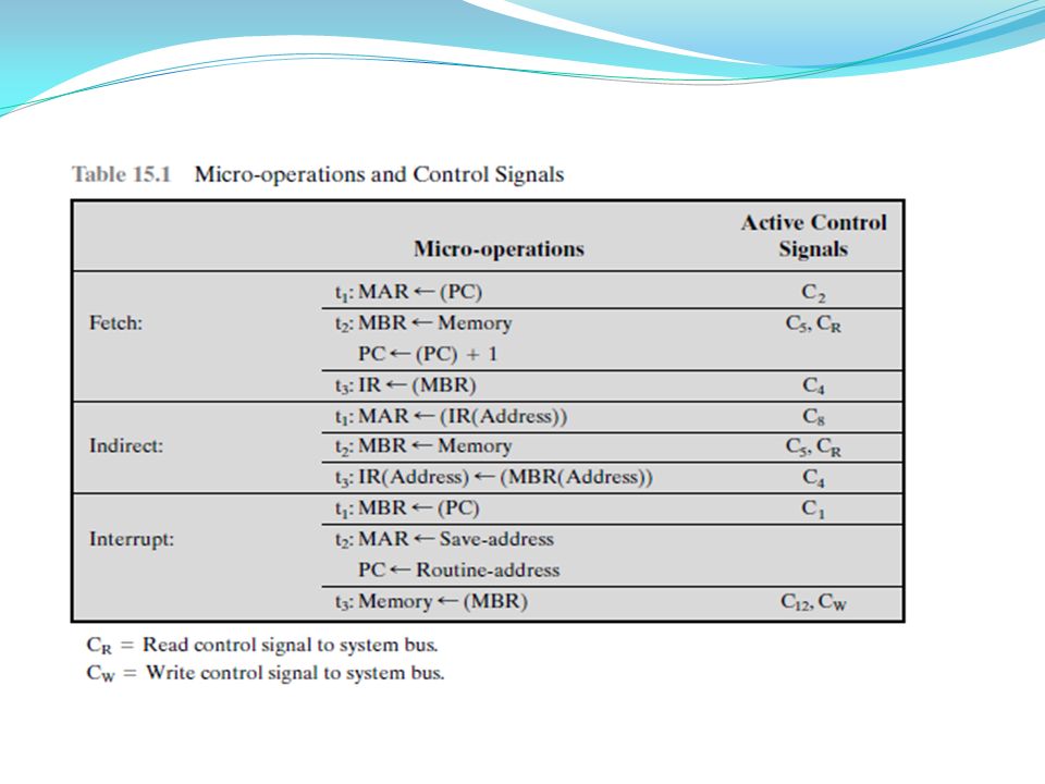
the simple fetch cycle actually consists of three steps and four micro-operations. Each micro-operation involves the movement of data into or out of a register. Symbolic Sequence : t1:MAR <- (PC) t2:MBR <- (memory) PC <- (PC) +I t3:IR <- (MBR) Where I = Instruction Length Each micro-operation can be performed within the time of a single time unit. The notation (T1,T2,T3)represents successive time units.
 t2:MBR <- (memory) PC <- (PC) +I t3:IR <- (MBR) Where I = Instruction Length Each micro-operation can be performed within the time of a single time unit. The notation (T1,T2,T3)represents successive time units..")
12
In words, we have First time unit: Move contents of PC to MAR. Second time unit: Move contents of memory location specified by MAR to MBR. Increment by I the contents of the PC. Third time unit: Move contents of MBR to IR.

13
Rules for Clock Cycle Grouping Proper sequence must be followed MAR <- (PC) must precede MBR <- (memory) Conflicts must be avoided Must not read & write same register at same time, because the results would be unpredictable. MBR <- (memory) & IR <- (MBR) must not be in same cycle Also: PC <- (PC) +1 involves addition Use ALU May need additional micro-operations
 & IR <- (MBR) must not be in same cycle Also: PC <- (PC) +1 involves addition Use ALU May need additional micro-operations.")
14
The Indirect Cycle Once an instruction is fetched, the next step is to fetch operands. let us assume a instruction format, with direct and indirect addressing. Symbolic Sequence : t1: MAR ← (IR(Address)) t2: MBR ← Memory t3: IR(Address) ← (MBR(Address)) The address field of the instruction is transferred to the MAR. This is then used to fetch the address of the operand.
) t2: MBR ← Memory t3: IR(Address) ← (MBR(Address)) The address field of the instruction is transferred to the MAR. This is then used to fetch the address of the operand..")
15
Interrupt Cycle At the completion of the execute cycle, a test is made to determine whether any enabled interrupts have occurred. If so, the interrupt cycle occurs. Symbolic Sequence : t1:MBR <-(PC) t2:MAR <- save-address PC <- routine-address t3:memory <- (MBR)
 t2:MAR <- save-address PC <- routine-address t3:memory <- (MBR).")
16
Execute Cycle for add The fetch, indirect, and interrupt cycles are simple and predictable. Each involves a small, fixed sequence of micro-operations and, in each case, the same micro-operations are repeated each time around. e.g. ADD R1,X add the contents of location X to Register 1, result in R1 t1:MAR <- (IR address ) t2:MBR <- (memory) t3:R1 <- R1 + (MBR) Note no overlap of micro-operations
 t2:MBR <- (memory) t3:R1 <- R1 + (MBR) Note no overlap of micro-operations.")
17
Execute Cycle for ISZ The content of location X is incremented by 1. If the result is 0, the next instruction is skipped ISZ X - increment and skip if zero t1:MAR <- (IR address ) t2:MBR <- (memory) t3:MBR <- (MBR) + 1 t4:memory <- (MBR) if (MBR) == 0 then PC <- (PC) + 1
 t2:MBR <- (memory) t3:MBR <- (MBR) + 1 t4:memory <- (MBR) if (MBR) == 0 then PC <- (PC) + 1.")
18
Execute Cycle for BSA BSA X - Branch and save address Address of instruction following BSA is saved in X Execution continues from X+1 t1:MAR <- (IR address ) MBR <- (PC) t2:PC <- (IR address ) memory <- (MBR) t3:PC <- (PC) + 1
 MBR <- (PC) t2:PC <- (IR address ) memory <- (MBR) t3:PC <- (PC) + 1")
19
Instruction Cycle Each phase decomposed into sequence of elementary micro-operations E.g. Fetch, Indirect, and Interrupt cycles Execute cycle One sequence of micro-operations for each op-code Assume new 2-bit register Instruction cycle code (ICC) designates which part of cycle processor is in 00: Fetch 01: Indirect 10: Execute 11: Interrupt
 designates which part of cycle processor is in 00: Fetch 01: Indirect 10: Execute 11: Interrupt.")
20
Flowchart for Instruction Cycle

21
CONTROL OF THE PROCESSOR Functional Requirements Define basic elements of processor Describe micro-operations processor performs Determine functions control unit must perform

22
Basic Elements of Processor ALU Registers Internal data paths Move Data Between (1) Reg. (2) Reg and ALU External data paths Move Data Between (1)Reg To Memory And I/O Modules Control Unit
 Reg and ALU External data paths Move Data Between (1)Reg To Memory And I/O Modules Control Unit.")
23
Types of Micro-operation Transfer data between registers Transfer data from register to external Transfer data from external to register Perform arithmetic or logical ops

24
Functions of Control Unit Sequencing Execution This is done using Control Signals

25
Control Signals Clock One micro-instruction (or set of parallel micro-instructions) per clock cycle Instruction register Op-code for current instruction Determines which micro-instructions are performed Flags State of CPU Results of previous operations From control bus Interrupts Acknowledgements
 per clock cycle Instruction register Op-code for current instruction Determines which micro-instructions are performed Flags State of CPU Results of previous operations From control bus Interrupts Acknowledgements")
26
block Diagram of Control Unit

27
Control Signals - output Within CPU Cause data movement Activate specific functions Via control bus To memory To I/O modules

28
Example Control Signal There is a simple processor with a single accumulator Control signals go to three separate destinations : Data paths: The control unit controls the internal flow of data. ALU: The control unit controls the operation of the ALU System bus: The control unit sends control signals

29
The control unit must have knowledge of where it is in the instruction cycle. Using this knowledge, and by reading all of its inputs, the control unit emits a sequence of control signals that causes micro-operations to occur. It uses the clock pulses to time the sequence of events

30
Data Paths and Control Signals

32
Internal Organization Usually a single internal bus Gates control movement of data onto and off the bus Control signals control data transfer to and from external systems bus Temporary registers needed for proper operation of ALU

33
CPU with Internal Bus ALU

34
Explain Hardwired implementation ? A wide variety of techniques have been used for control unit implementation : Two categories: In a hardwired implementation, the control unit is essentially a state machine circuit Micro-programmed implementation Control Unit Inputs Control Unit logic

35
Hardwired Implementation Control unit inputs Flags and control bus Each bit means something Instruction register Op-code causes different control signals for each different instruction Unique logic for each op-code Decoder takes encoded input and produces single output n binary inputs and 2 n outputs

36
Hardwired Implementation (2) Clock Repetitive sequence of pulses Useful for measuring duration of micro-ops Must be long enough to allow signal propagation Different control signals at different times within instruction cycle Need a counter with different control signals for t1, t2 etc.
 Clock Repetitive sequence of pulses Useful for measuring duration of micro-ops Must be long enough to allow signal propagation Different control signals at different times within instruction cycle Need a counter with different control signals for t1, t2 etc.")
37
Control Unit with Decoded Inputs

38
Control Unit logic Let us consider a single control signal, C5.This signal causes data to be read from the external data bus into the MBR. Let us define two new control signals, P and Q, that have the following interpretation: PQ = 00 Fetch Cycle PQ = 01 Indirect Cycle PQ = 10 Execute Cycle PQ = 11 Interrupt Cycle Then the following Boolean expression defines C5: C5 = P.Q.T2 + P.Q.T2 That is, the control signal C5 will be asserted during the second time unit of both the fetch and indirect cycles.

39
This expression is not complete. C5 is also needed during the execute cycle. For our simple example, let us assume that there are only three instructions that read from memory: LDA,ADD, and AND. Now we can define C5 as C5 = P. Q. T2 + P. Q. T2 + P. Q. (LDA + ADD + AND). T2
. T2.")
Similar presentations


 Processor Internals CHAPTER 15: CONTROL UNIT OPERATION 1.>")


