Download presentation
Presentation is loading. Please wait.

1
General detectors

2
CCDs Charge Coupled Devices invented in the 1970s Sensitive to light from optical to X-rays In practice, best use in optical and X-rays CCDs make use of silicon chips The CCD consists of (1) a p-type doped silicon substrate, (2) the charge storage (depletion) layer, which is covered by (3) a SiO2 insulating layer; upon this is (4) an array of closely spaced electrodes, which can be set to pre-defined voltage value
 a p-type doped silicon substrate, (2) the charge storage (depletion) layer, which is covered by (3) a SiO2 insulating layer; upon this is (4) an array of closely spaced electrodes, which can be set to pre-defined voltage value")
3
Si array p-type Si array n-type Also Sb,P Also Al,Ga

4
Electrons in a lattice do not have discrete energies. They form energy bands: Valence band Conduction band For semi-conductors, the Fermi level is just in the middle of the conduction and valence bands. At finite temperature, some electrons of the valence band can jump into the conduction band (current noise) E G (Si)=1.1 eV (IR), E G (Ge)=0.72 eV E G (C)=5.5 eV (insulator) Reminder of solid state physics photon Hole Electron (From http://hyperphysics.phy-astr.gsu.edu/hbase/hframe.html)http://hyperphysics.phy-astr.gsu.edu/hbase/hframe.html
 E G (Si)=1.1 eV (IR), E G (Ge)=0.72 eV E G (C)=5.5 eV (insulator) Reminder of solid state physics photon Hole Electron (From")
5
The pn junction

6
Forward-biased pn junction Reverse-biased pn junction

7
Transverse cut of CCD with buried channel Blecha (cours instrumentation) 4.1 eV 2.5 eV 1.8 eV 1.2 eV
 4.1 eV 2.5 eV 1.8 eV 1.2 eV")
8
The electrode has positive potential to attract the generated photoelectrons in a potential well The above MOS capacitor is 1 pixel

9
Front-illuminated CCDs p Incoming photons 625 m n They have a low Quantum Efficiency due to the reflection and absorption of light in the surface electrodes. Very poor blue response. The electrode structure prevents the use of an anti-reflective coating that would otherwise boost performance. Incoming photons 15 m n p Anti-reflective coating The QE can approach 100%. These thinned CCDs become transparent to near infra-red light and the red response is poor. Response can be boosted by the application of an anti- reflective coating on the thinned rear-side. These coatings do not work so well for front- illuminated CCDs due to the surface bumps created by the surface electrodes Courtesy of S. Tulloch

10
Quantum Efficiency Comparison The graph below compares the quantum of efficiency of a thick frontside illuminated CCD and a thin backside illuminated CCD. Courtesy of S. Tulloch

11
Back-illuminated CCDs Thinner deadlayers higher low-E QE Thinner active region lower high-E QE Increased noise, charge transfer inefficiency higher FWHM BI CCD FI CCD From C. Grant, X-ray Astronomy School 2007

12
Structure of a CCD One pixel Channel stops to define the columns of the image Transparent horizontal electrodes to define the pixels vertically. Also used to transfer the charge during readout Plan View Cross section The diagram shows a small section (a few pixels) of the image area of a CCD. This pattern is reapeated. Electrode Insulating oxide n-type silicon p-type silicon Every third electrode is connected together. Bus wires running down the edge of the chip make the connection. The channel stops are formed from high concentrations of Boron in the silicon. Courtesy of S. Tulloch
 of the image area of a CCD. This pattern is reapeated. Electrode Insulating oxide n-type silicon p-type silicon Every third electrode is connected together. Bus wires running down the edge of the chip make the connection. The channel stops are formed from high concentrations of Boron in the silicon. Courtesy of S. Tulloch.")
13
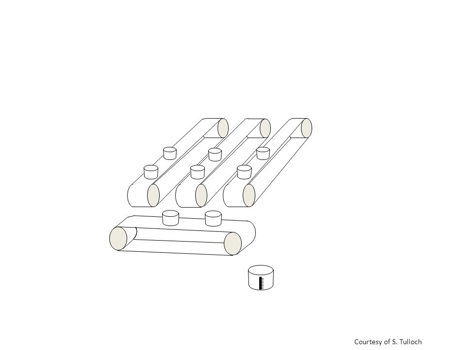
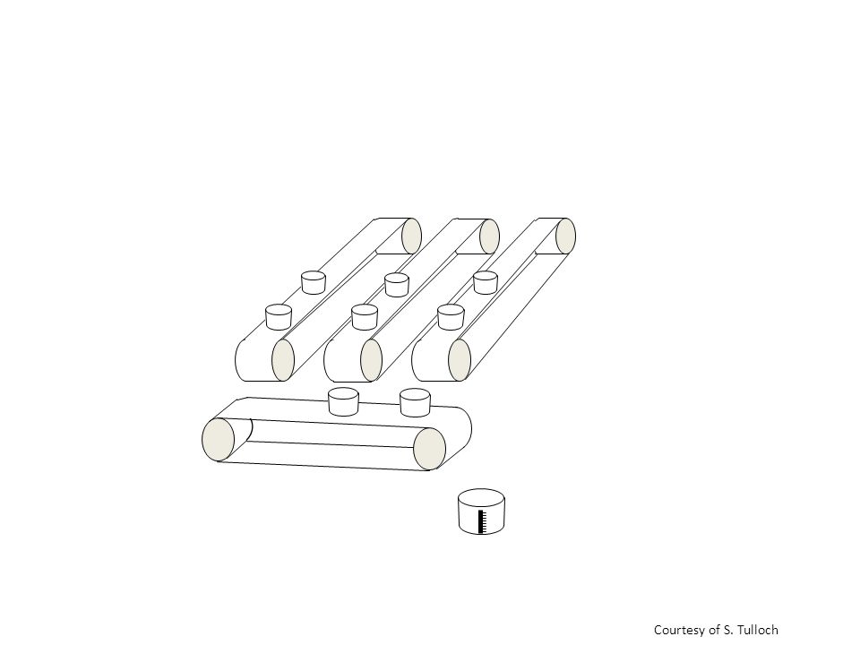
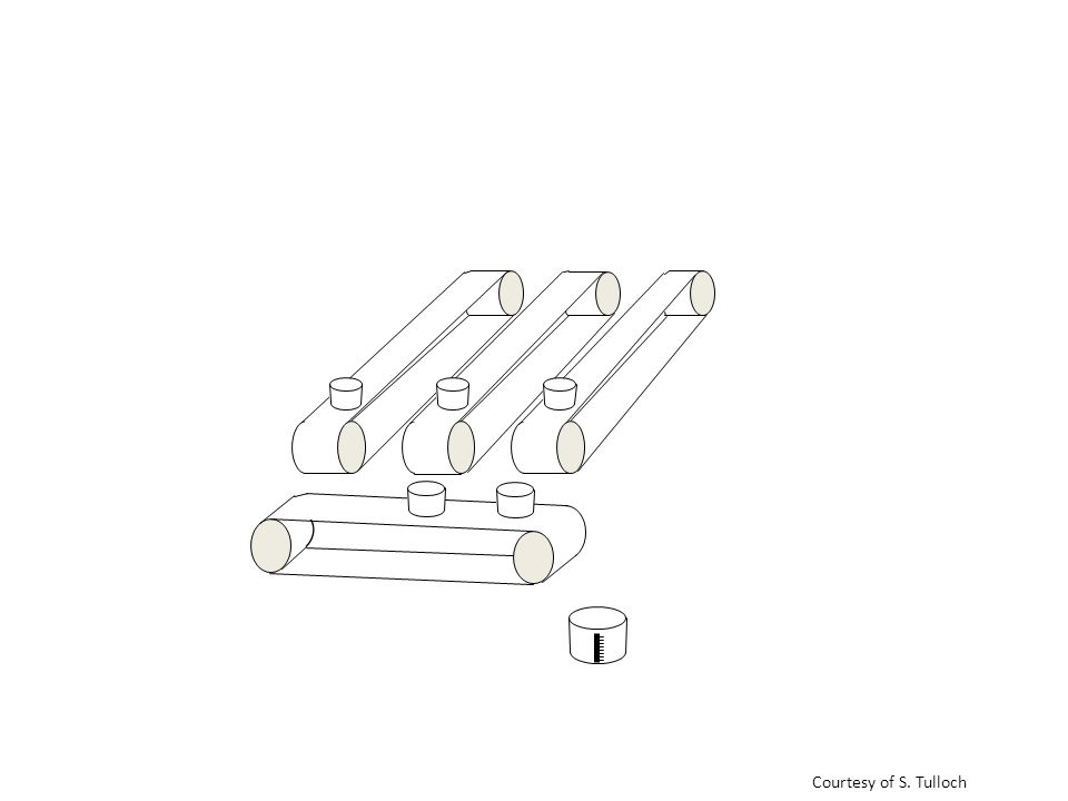
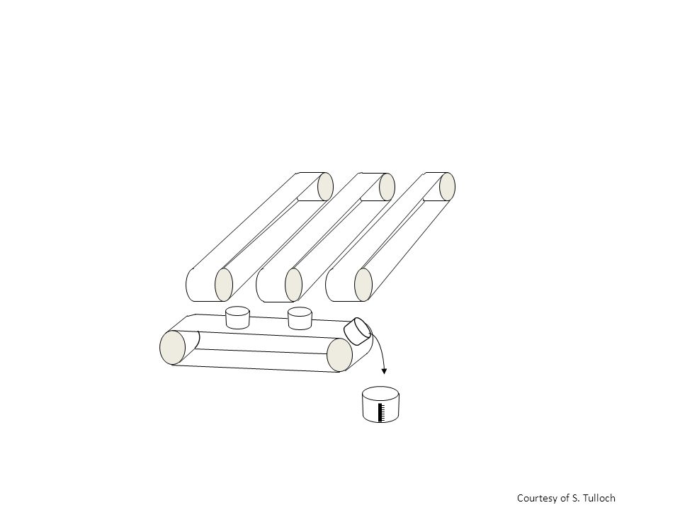
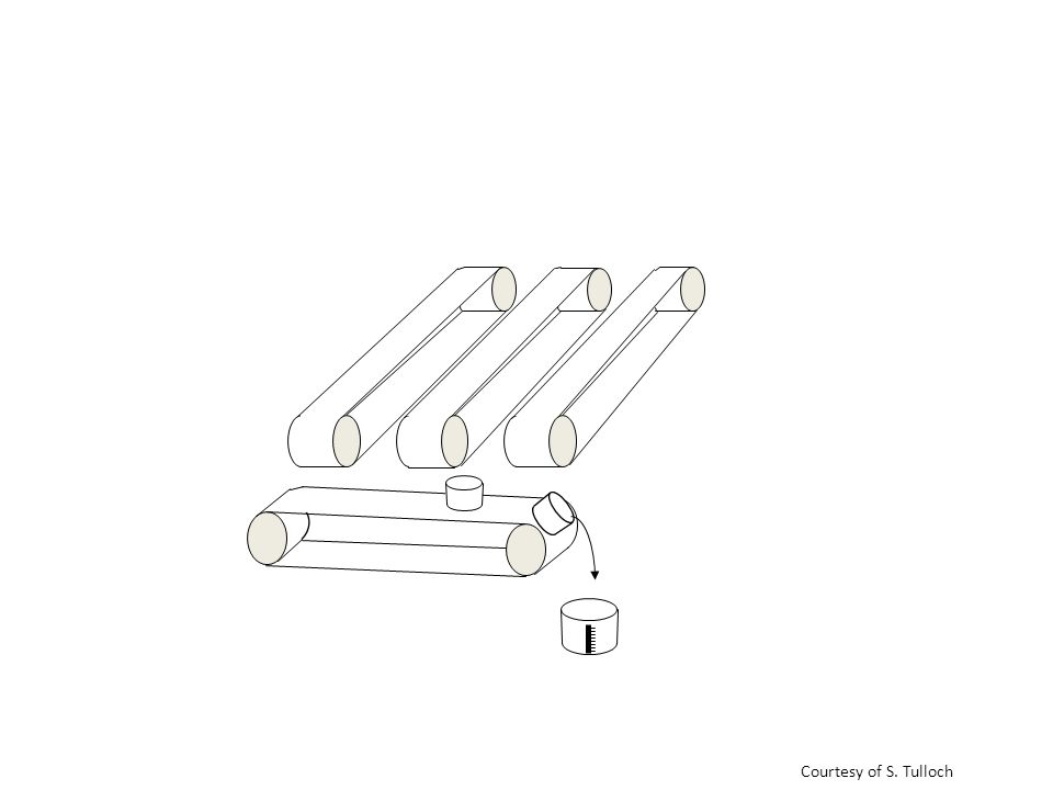
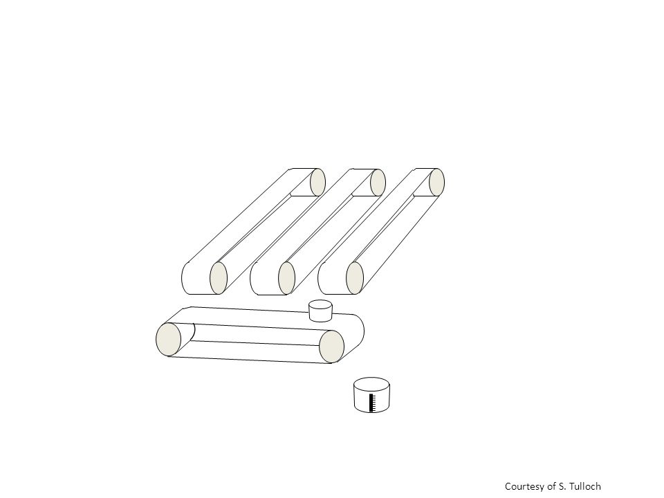
RAIN (PHOTONS) BUCKETS (PIXELS) VERTICAL CONVEYOR BELTS (CCD COLUMNS) HORIZONTAL CONVEYOR BELT ( SERIAL REGISTER ) MEASURING CYLINDER (OUTPUT AMPLIFIER) CCD Analogy Courtesy of S. Tulloch

14
Exposure finished, buckets now contain samples of rain. Courtesy of S. Tulloch

15
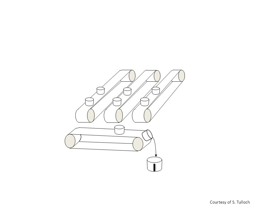
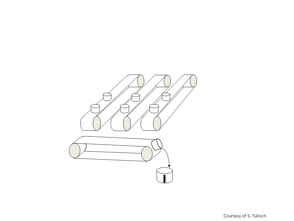
Conveyor belt starts turning and transfers buckets. Rain collected on the vertical conveyor is tipped into buckets on the horizontal conveyor. Courtesy of S. Tulloch

16
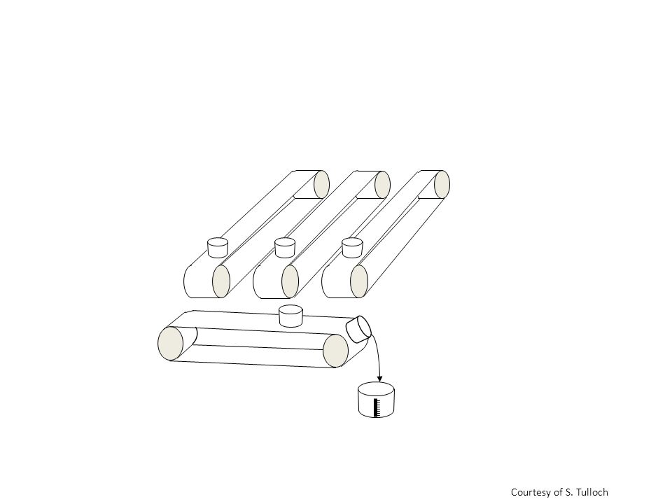
Vertical conveyor stops. Horizontal conveyor starts up and tips each bucket in turn into the measuring cylinder. Courtesy of S. Tulloch

17
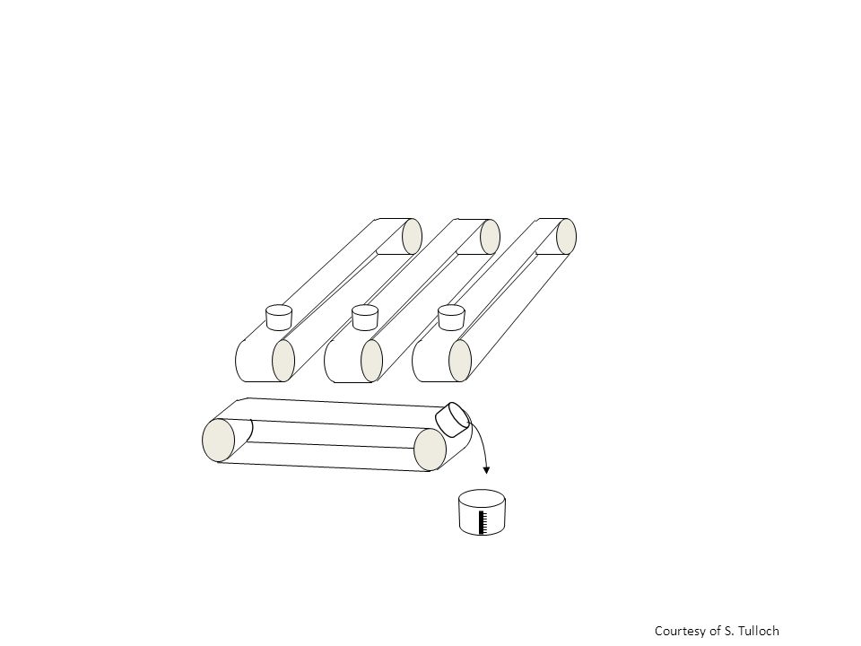
` After each bucket has been measured, the measuring cylinder is emptied, ready for the next bucket load. Courtesy of S. Tulloch

24
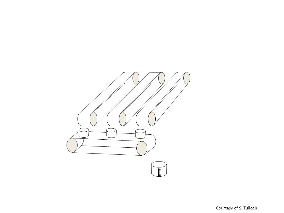
A new set of empty buckets is set up on the horizontal conveyor and the process is repeated. Courtesy of S. Tulloch

41
Eventually all the buckets have been measured, the CCD has been read out. Courtesy of S. Tulloch

42
pixel boundary Charge packet p-type silicon n-type silicon SiO2 Insulating layer Electrode Structure pixel boundary incoming photons Charge Collection in a CCD. Photons entering the CCD create electron-hole pairs. The electrons are then attracted towards the most positive potential in the device where they create ‘charge packets’. Each packet corresponds to one pixel Courtesy of S. Tulloch

43
Charge Transfer in a CCD 1. In the following few slides, the implementation of the ‘conveyor belts’ as actual electronic structures is explained. The charge is moved along these conveyor belts by modulating the voltages on the electrodes positioned on the surface of the CCD. In the following illustrations, electrodes colour coded red are held at a positive potential, those coloured black are held at a negative potential. 1 2 3 Courtesy of S. Tulloch

44
1 2 3 +5V 0V -5V +5V 0V -5V +5V 0V -5V Time-slice shown in diagram 1 2 3 Charge Transfer in a CCD 2. Courtesy of S. Tulloch

45
1 2 3 +5V 0V -5V +5V 0V -5V +5V 0V -5V 1 2 3 Charge Transfer in a CCD 3. Courtesy of S. Tulloch

46
1 2 3 +5V 0V -5V +5V 0V -5V +5V 0V -5V 1 2 3 Charge Transfer in a CCD 4. Courtesy of S. Tulloch

47
1 2 3 +5V 0V -5V +5V 0V -5V +5V 0V -5V 1 2 3 Charge Transfer in a CCD 5. Courtesy of S. Tulloch

48
1 2 3 +5V 0V -5V +5V 0V -5V +5V 0V -5V 1 2 3 Charge Transfer in a CCD 6. Courtesy of S. Tulloch

49
1 2 3 +5V 0V -5V +5V 0V -5V +5V 0V -5V 1 2 3 Charge Transfer in a CCD 7. Charge packet from subsequent pixel enters from left as first pixel exits to the right. Courtesy of S. Tulloch

50
1 2 3 +5V 0V -5V +5V 0V -5V +5V 0V -5V 1 2 3 Charge Transfer in a CCD 8. Courtesy of S. Tulloch

51
Photomultipliers Gain of 10 7 -10 9 From Bruker-AXS

52
Semi-conductor detectors See introduction on semiconductors in previous slides (conduction/valence bands) Gamma-ray interaction produces secondary electrons; they produce electron-hole pairs in the conduction/valence bands Electric field separates the pairs before recombination, drifting electrons to anode and holes to cathode. Charge is collected, which is proportional to energy deposited in detector Energy required to generate electron-hole pair is =(14/5)E g +c, where 0.5≤c≤ eV Common detectors made of Ge (e.g., Integral SPI; E g =0.74 eV, =2.98 eV), Si ( =3.61 eV), CdTe (Integral ISGRI; E g =1.6eV, =4.43 eV)
E g +c, where 0.5≤c≤ eV Common detectors made of Ge (e.g., Integral SPI; E g =0.74 eV, =2.98 eV), Si ( =3.61 eV), CdTe (Integral ISGRI; E g =1.6eV, =4.43 eV).")
53
Bolometer principles Sensitive to energy Not sensitive to ‘color’ Suited for almost ANY wavelength Particularly suited for IR and FIR to sub-mm (but cooling to mK required)
")
54
Bolometer priciples

55
Bolometers

Similar presentations


 AS3100 Lab. Astronomi Dasar I Prodi Astronomi 2007/2008 B. Dermawan.>")


 BUCKETS (PIXELS) VERTICAL CONVEYOR BELTS (CCD COLUMNS) HORIZONTAL CONVEYOR BELT ( SERIAL REGISTER ) MEASURING CYLINDER (OUTPUT AMPLIFIER)>")


>")

.>")

