Download presentation
Presentation is loading. Please wait.

1
EE 3755 Datapath Presented by Dr. Alexander Skavantzos

3
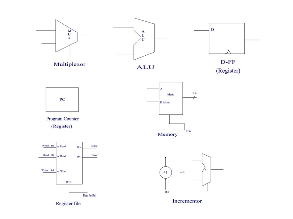
#Program Counter Why just increment 1? “Because of Alignment” “Every instruction is 4 bytes long.”

4
How to Implement ADD Instruction to work?

6
Where the “ADD” control signal for ALU comes? “From the instruction field ‘5-0’ [function field] and OPCode (31-26)”
 .")
7
Can the above H/W perform ADDi instructions? What do we need?

8
We need to get the immediate data, and “RT” field becomes acting like destination field at “R” format. ADDi rt, rs, imm

9
Where the “CNT” signal come? “From the OPCode field (31-26)”
")
10
(Probably not work due to fan-out)
")
11
“Can the above H/W perform OR Instruction?” “Do we need more H/W?”

12
It also can perform “ORi” without having more H/W.

13
So far we don’t have any instructions to access memory and we don’t have data memory unit yet. How to implement this? And what will be ALU operation?

14
One way to do this is using the ALU to compute memory address and put the output of ALU (computed memory address; (R9+8)) to the address of memory and put the data from the memory register file (R7). Can we do this? Memory output should go back to register file and ALU output should go back to register file.

15
But this time ALU output is memory address and D out is data. This is a collision. How can we solve this? => Multiplexor Where the CNTMUX come? => If “LW” instruction, then the mux should select input from memory. => So, from Control Signal.

16
Can the above H/W perform “LB”? What will be problems? How can you modify above H/W to perform “LB”?

17
LB is loading only one byte and L is loading 4 bytes. So we have to think about either modifying memory unit (Memory Module) to get one byte data at a time (LW, we assume the memory unit giving us 4 bytes data). So let’s assume the memory unit giving us 4 bytes data, then we have to truncate extra 3 bytes data, and we have to think about memory address. If we assume we could access arbitrary memory address, then we need logic to do that.
 to get one byte data at a time (LW, we assume the memory unit giving us 4 bytes data). So let’s assume the memory unit giving us 4 bytes data, then we have to truncate extra 3 bytes data, and we have to think about memory address. If we assume we could access arbitrary memory address, then we need logic to do that..")
18
We need logic to truncate extra 3 bytes data and memory address logic to access arbitrary address (Alignment problem). So when we perform “LBU,” truncation logic will give us byte data with 20 zeroes padded to upper part. So we could make TRUC_CNT and MEM_CNT from Control Signal. It (LBU) can be done with above H/W. But think about “SB.” Can “SB” be done with above approach?
 can be done with above H/W. But think about SB. Can SB be done with above approach .")
19
TRUNCATE LOGIC But because of alignment problem and accessing arbitrary address the logic will be complicated. The above logic is working when accessing “0000” but what about accessing “0001”?

20
The problem of SB is we are saving only one byte out of 4 bytes. So we have to think about how to save data to the memory. For SW, if we assume can save 4 bytes by giving an address, SW will be easily implemented.

21
Can “SB” be done with above “HW”?Can we remove the new datapath? Can we just by pass through ALU?

22
When we cover Verilog, we implement ALU unit. It can perform “ADD,” “SUBTRACTION,” “SLT,” “AND,” “OR,” “ByPassA” and “ByPassB.” So, we could bypass Drt value through ALU, we can remove the new datapath. BUT, The Answer is NO. No, ALU is performing Address calculation (RS + offset). So, we can not bypass this time. Then we need the new datapath.
. So, we can not bypass this time. Then we need the new datapath..")
23
Again, even we can perform SW, doing “SB” is not OK. For “LB,” we could use “LW” and then truncate some bits (24 bits). But for “SB” case, we can not do that. One way of doing that is “LW” and modifying byte information and using “SW.” But this brings extra “LW.” So, we may assume that we could store byte and for SW instruction, we assume we could store 4 bytes. Then we need control circuit between Drt and Din.
. But for SB case, we can not do that. One way of doing that is LW and modifying byte information and using SW. But this brings extra LW. So, we may assume that we could store byte and for SW instruction, we assume we could store 4 bytes. Then we need control circuit between Drt and Din..")
25
Do we need extra datapath to perform Slt? Do we need extra H/W to perform Slt? Can the above H/W perform “SLTi”?

27
Ox1000: BEQ R10, R11, 12 What will be the target address? How to compute the target address? BEQ rs, rt, label What kind of action do we need? a) compute the target address b) Check the branch condition (rs=rt) Action a) needs Addition Action b) needs Addition [Subtraction]
 compute the target address b) Check the branch condition (rs=rt) Action a) needs Addition Action b) needs Addition [Subtraction].")
28
Target Address PC + 4 + offset * 4 [12] 1100 0*1004 [12*4] 11 0000 ox3 0 1004 + 30 ox1034 [Target address] a) b)
![Target Address PC offset * 4 [12] *1004 [12*4] ox ox1034 [Target address] a) b)](http://images.slideplayer.com/28/9386520/slides/slide_28.jpg "Target Address PC offset * 4 [12] *1004 [12*4] ox ox1034 [Target address] a) b)")
29
Target Address Computation logic:Added Branch condition logic:Added Multiplexor for PC+4 and Target address:Added What’s wrong with this? (What if an instruction perform subtraction and the result is zero; what will be the next address to fetch).
..")
30
Can the previous page H/W perform “BNE”? a) computing target address b) computing branch condition
 computing target address b) computing branch condition")
31
Is this logic OK with Delayed Branch?

32
If branch condition is true, the next instruction to be executed is the branch target, instead of PC+4. So, we need to change the H/W. <=

33
Target address computation {pc [31:28], target, 00} 10000000 + 2000*4 =10008000 target address
![Target address computation {pc [31:28], target, 00} *4 = target address](http://images.slideplayer.com/28/9386520/slides/slide_33.jpg "Target address computation {pc [31:28], target, 00} *4 = target address")
34
Target address computation {pc [31:28], target, 00} 10000000 + 2000*4 =10008000 target address 0x10000000 jr 0x2000 0001 0000 0000 0000 0000 0000 0000 0000 (pc) take 0001 (pc[31:28]) 4bits take 00 0000 0000 0010 0000 0000 0000 (target) 26bits. 0001 00 0000 0000 0010 0000 0000 0000 00(padding 2 zeros) 0001 00 0000 0000 0010 0000 0000 0000 00 0001 0000 0000 0000 1000 0000 0000 0000 (rearrange) 0X 1 0 0 0 8 0 0 0 (target address)
![Target address computation {pc [31:28], target, 00} *4 = target address 0x jr 0x (pc) take 0001 (pc[31:28]) 4bits take (target) 26bits.](http://images.slideplayer.com/28/9386520/slides/slide_34.jpg "(padding 2 zeros) (rearrange) 0X (target address).")
35
JUMP “Can the above H/W perform jr R10?”

36
Jr R10; Jr Rs Target address is in R10. So we need a datapath from D/rs to NPC. The “Control” comes from bit 31-26 and bit 5-0

37
“Jr Rs” If we want to perform jal, what do we need more?

38
For Jal instruction, everything is the same as j instruction, except, we have to save NPC to “R31.” Jal ox2000

39
So we need datapath to D/In from NPC and datapath to A Write to point ra (r31) This way, we could save PC+8 to ra. The control and CNT signals can be coming from Control logic.

40
“jal ox2000” “Added H/W for saving R31”

41
“Jalr Rs, Rd” Instruction. Everything is same to jr rs instruction, except we have to save the return address to “rd.” Jalr R10, R11 Do we need new datapath?

42
“jalr R10, R11 We don’t need new datapath

Similar presentations


>")


 Fall 2007 Lecture 10: Instruction Representation II.>")
>")


 FETCH = Read the instruction.>")


 Lecture 9: Assemblers, Linkers, and Loaders * Jeremy R. Johnson Mon. April 23,>")

