Download presentation
Presentation is loading. Please wait.

1
Lesson Plan: How small am I? The Science of Nanotechnology RET Teacher: Efremfon F. Ekpo Bethune Cookman College Professor : Ashok Kumar Subjects : Nanotechnology, Physical Science, General Physics Time : Two class periods (approximately 120 minutes) Target Group: College students(Physical Science class). 2006 RET Lesson Plan
 Target Group: College students(Physical Science class) RET Lesson Plan.")
2
Nanotechnology is the manipulation of matter at a scale of 1 to 100 nanometers. Using nanotechnology we can control molecules at an atomic level and create materials with unique properties. A nanometer is 10-9 (a billionth) of a meter. The prefix nano is Greek for dwarf. As a reference point, a hair is approximately 100,000 nanometers. A red blood cell is approximately 10,000 nanometers. Introduction
 of a meter. The prefix nano is Greek for dwarf. As a reference point, a hair is approximately 100,000 nanometers. A red blood cell is approximately 10,000 nanometers. Introduction.")
3
Fundamentally the properties of materials can be changed by nanotechnology. We can arrange molecules in a way that they do not normally occur in nature. The material strength, electronic and optical properties of materials can all be altered using nanotechnology. Introduction

4
See diagram below. Source: www.nbtc.cornell.edu and images from www.denniskunkel.com Figure 1. Size Scale Introduction

5
Lesson Objectives Students will gain an understanding of nanoscale dimensions. Students will gain an understanding nanotechnology. Students will understand the importance of nanotechnology.

6
Materials: How small am I ? gamegame Liquid soap Water Small bowls Straws Simple complex lenses (optional)
.")
7
Procedures 1. Check for prior learning. Ask the students the following questions: What does nano mean? (Answer: a billionth) What, then, is a nanometer? (Answer: a billionth of a meter)
 What, then, is a nanometer. (Answer: a billionth of a meter).")
8
Click here for the game board. Cut out the squares on the board into cards so each card has an image. Each student pair receives a set of cards and arranges the small objects into size order, biggest to smallest. The teacher then checks for accuracy and discusses size of each object. Have students arrange small objects into correct order from biggest to smallest. (Answer: The order should be: hair, red blood cell, bacterium, dust particle, wavelength of red light, wavelength of ultraviolet light, computer chip wire, helix of DNA, carbon atom ) game board 2. New learning. Ask students: How small is a nanometer? (For Answer: Play the “How Small Am I?” game)game
 game board 2. New learning. Ask students: How small is a nanometer. (For Answer: Play the How Small Am I game)game.")
9
Discuss with the students how small a micrometer is and what the size of relatively common objects are in micrometers. CAN WE DEFINE MICROMETER HERE ? (Example: a human hair is approximately 100 micrometers in width. In the microscopic world, a red blood cell is approximately 10 micrometers, while your average bacterium is approximately 1 micron, OR DEFINE MICRON HERE, in width. Some features in a computer chip are less than 1/10 of a micrometer or about 1/1000th the width of your hair. A nanometer is 10-9 (a billionth of a meter.) How small am I?
 How small am I .")
10
[MAYBE A VISUAL WOULD BE GOOD HERE: SHOW EACH TERM FROM THE SMALLEST TO BIGGEST AND SHOW OBJECTS WITH NUMBERS BELOW OBJECTS -- GREAT FOR VISUAL LEARNERS] How small am I?
![[MAYBE A VISUAL WOULD BE GOOD HERE: SHOW EACH TERM FROM THE SMALLEST TO BIGGEST AND SHOW OBJECTS WITH NUMBERS BELOW OBJECTS -- GREAT FOR VISUAL LEARNERS] How small am I](http://images.slideplayer.com/24/7504877/slides/slide_10.jpg "[MAYBE A VISUAL WOULD BE GOOD HERE: SHOW EACH TERM FROM THE SMALLEST TO BIGGEST AND SHOW OBJECTS WITH NUMBERS BELOW OBJECTS -- GREAT FOR VISUAL LEARNERS] How small am I")
11
Engage the students to make predictions of what the size of some objects might be when measured in nanometers. Ask the students to imagine how they might arrange molecules in a highly precise manner. How small am I?

12
Nanotechnology is the manipulation of matter at a scale of 1 to 100 nanometers. The challenge is to move molecules and arrange them precisely. There are basically three different means to manipulate matter at a scale of 1 to 100 nanometers. Pick them up and move them Pattern them (lithography) Use self-assembly How small am I?
 Use self-assembly How small am I .")
13
Strange but true, you can pick molecules up and move them. The ‘tool’ used to move them is an atomic force microscope (AFM). It is a microscope in that it can ‘see’ by measuring the attractive forces between a sample and a very sharp tip. 1.Pick them up and move them
. It is a microscope in that it can ‘see’ by measuring the attractive forces between a sample and a very sharp tip. 1.Pick them up and move them.")
14
As the tip moves along the surface it ‘sees’ by measuring the attraction or repulsion between the tip and the surface. The tip is mounted on a cantilever (like a diving board) and the movement of the cantilever is measured by bouncing a laser beam off the surface of the cantilever. An AFM can measure differences as small as 1/10 of a nanometer.
 and the movement of the cantilever is measured by bouncing a laser beam off the surface of the cantilever. An AFM can measure differences as small as 1/10 of a nanometer..")
15
AFM Tip Source: www.nanoscience.com, monet.physik.unibas.ch/famars/statanim.htmwww.nanoscience.com Figure 2 Figure 3

16
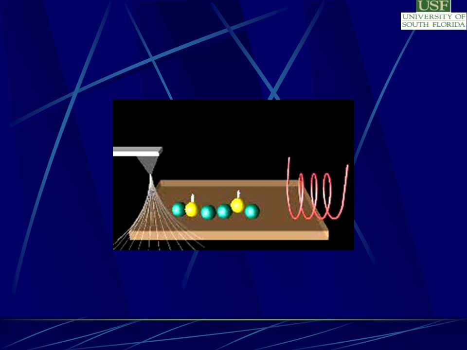
The tip of an AFM can also be used to move a molecule if you can figure out how to ‘pick up’ and then release the molecule. This is one of the more famous ‘real’ images of nanotechnology. AFM Tip

17
In the mid-1980’s, IBM spelled their logo using thirteen xenon atoms. Each atom was picked up using an AFM tip and moved into place. While the picture suggests a very nice stable arrangement the atoms were in fact continuously moving and the ‘letters’ were short lived. AFM Tip Figure 4. IBM logo spelled out with xenon atoms Source: www-306.ibm.com/chips/periodic/xe-a.html

18
What is this figure?

20
All nanometer sized electronic components are made using a process called lithography. Alois Senefelder of Munich discovered the basic principle of lithography, “printing on stone”, around 1798. It is based upon the notion that oil and water do not mix. So patterns can be made on a surface by drawing with an oily substance (like a crayon), and only where the oily substance is not present will a water-based ink adhere. 2. Pattern them (lithography)
, and only where the oily substance is not present will a water-based ink adhere. 2. Pattern them (lithography).")
21
You can also cover the entire surface scribbling with a crayon and then scratch away to ‘draw’ your pattern. Craft people call this type of material scratch boards. The key in nanotechnology is to ‘draw’ with very fine resolution. 2. Pattern them (lithography)
.")
22
Ask if any students have a mechanical pencil or a pen that has a specified line width. The finest mechanical pencils draw a line that is 0.5 millimeters. That is 500 microns or about 1,000 times wider than the wires inside of a computer chip. 2. Pattern them (lithography)
.")
23
Photolithography involves using energy (e.g., light or electrons) to change the solubility of a material. Photolithography literally means light-stone-writing in Greek. An image can be produced on a surface by drawing with light or electrons much the same way that you might scratch away the crayon on a scratch board. 2. Pattern them (lithography)
.")
24
Ask the students to think of some process that involves light and causes a chemical change. Two processes that come to mind are sun tanning and photography. Both involve a chemical that is changed by exposure to light. 2. Pattern them (lithography)
.")
25
Ask students to think about how both sun tanning and photography work and discuss the differences. 2. Pattern them (lithography)
.")
26
Both involve a chemical change that is triggered by light. With sun tanning, the light is mostly ultraviolet and the reaction involves cells that are stimulated by sun light producing a pigment. 2. Pattern them (lithography)
.")
27
The pigment, melanin, is produced to protect cells against damage due to sunlight. In photography, tiny silver crystals in the film are reactive to different wavelengths of visible light and produce the variety of colors. 2. Pattern them (lithography)
.")
28
Back to nanotechnology and photolithography. In nanotechnology we use photolithography to transfer a pattern from a ‘mask’ to a surface. We apply a special chemical called ‘photoresist’, which is sensitive to light, onto the surface that we want to pattern. The mask is a stencil which allows the light energy to pass through only certain regions. 2. Pattern them (lithography)
.")
29
So a pattern on a mask can be transferred to a surface by passing light or electrons through the mask. When the light or the electrons reach the photoresist on the surface, the solubility of the photoresist changes making it easier or harder to wash away. What is left after washing is the three-dimensional pattern that was originally on the mask. It is transferred to the photoresist. 2. Pattern them (lithography)
.")
30
Figure 5. Mask used to transfer a pattern onto a surface www.nbtc.cornell.edu 2. Pattern them (lithography)
.")
31
The limitation in resolution is how small a beam of light or electrons can be produced. Ask the students how they might make an object smaller. If they seem puzzled ask them how they would shrink an image. 2. Pattern them (lithography)
.")
32
The answer is using a series of lenses. If you have a simple convex lens, hold it up and project the image of a light from the ceiling on to a piece of paper (fluorescent lights work fine). The image of the light will shrink. If you put a lens between the mask and the surface, the image that passes through the lens is shrunken when projected on the surface 2. Pattern them (lithography)
. The image of the light will shrink. If you put a lens between the mask and the surface, the image that passes through the lens is shrunken when projected on the surface 2. Pattern them (lithography).")
33
Figure 5. Lenses and light used to shrink images Scientists use photolithography to make computer chips and other devices that have very small features, as small as 100 nanometers. foodmicro.foodsci.cornell.edu/fmlab/personnel/cady.htm 2. Pattern them (lithography)
.")
34
Figure 6. Surface that is patterned using photolithography www.nbtc.cornell.edu 2. Pattern them (lithography)
.")
35
Snow flakes Salt crystals Soap bubbles 3.Use self-assembly Ask students to think of an example where molecules arrange themselves into a pattern.

36
Molecules self-assemble when the forces between these molecules are sufficient to overcome entropy. Entropy is what drives molecules to a low energy state. 3.Use self-assembly

37
Snowflakes form in patterns because of the nanoscale arrangement of the water molecules. Snowflakes form around nanoscale particles of dirt that nucleate ice crystals. As the temperature approaches the freezing point of water, the hydrogen bonds between water molecules arrange the water into a crystal pattern that grows. 3.Use self-assembly

38
Salt will assemble to form crystals. Salt crystals form as the salt molecules arrange themselves while the water evaporates. The bonds between the salt molecules are strong enough to squeeze out the water and arrange themselves to form a crystal. 3.Use self-assembly

39
The different geometries of the salt molecules affect the shape of the salt crystals, so the nanoscale geometry affects the macroscale appearance of the crystal. 3.Use self-assembly

40
The soap molecules form two layers that sandwich a layer of water in between. This is because the soap molecules have one end that likes water and one that does not. So the end that does not like water is on the outside and the other end that likes the water is on the inside. 3.Use self-assembly Soap bubbles self-assemble

41
The soap forms a monolayer on the inside and a monolayer on the outside of the water. Each layer of soap is a self-assembled monolayer, a single layer of molecules oriented in one direction. It is also flexible, which results in changes in the appearance (e.g., color, reflectivity) of the soap bubble. 3.Use self-assembly
 of the soap bubble. 3.Use self-assembly.")
42
Soap bubbles self-assemble. The soap molecules form two layers that sandwich a layer of water in between. This is because the soap molecules have one end that likes water and one that does not. So the end that does not like water is on the outside and the other end that likes the water is on the inside. 3.Use self-assembly

43
The soap forms a monolayer on the inside and a monolayer on the outside of the water. Each layer of soap is a self-assembled monolayer, a single layer of molecules oriented in one direction. It is also flexible, which results in changes in the appearance (e.g., color, reflectivity) of the soap bubble. 3.Use self-assembly
 of the soap bubble. 3.Use self-assembly.")
44
The students should see a few things. One thing to observe is the color, which appears almost like a rainbow. Why do the colors look like a rainbow? White light is composed of all the visible colors. The light passing through the bubble creates a phenomenon called interference. The colors in a bubble appear because light is reflected from both the inside and the outside of the bubble at the same time. 3.Use self-assembly Have students blow a soap bubble and observe it.

45
The bubble is so thin that the light reflected from the outside is either enhanced or canceled out by the light reflected from the inside. When the two sets of reflected waves are combined, they can remove or reinforce various wavelengths of light thus enhancing some colors and suppressing others. All of this happens because the distance between the outer and inner layer of the bubble is approximately 150 nanometers, about 1/1,000 the width of a hair. 3.Use self-assembly

46
Figure 7. Soap bubble schematic home.earthlink.net/~marutgers/science/soapbasics/gifs/bubble.gif 3.Use self-assembly

47
Have students repeat the “How small am I ?” game. Discuss as a group the scale at which the bubble molecules interacted with the water molecules. The interactions within the bubble occur at a scale that is smaller than the wavelength of light. Scientists can make tiny structures such as the wires in a computer chip that are smaller than the wavelength of light. Check for learning

48
Extension activities Sunprint paper and photolithography (www.nbtc.cornell.edu/mainstreetscience/lessons.html)www.nbtc.cornell.edu/mainstreetscience/lessons.html Nanosmores and photolithography (www.nbtc.cornell.edu/mainstreetscience/lessons.html)www.nbtc.cornell.edu/mainstreetscience/lessons.html Reduction from bulk to nanoscale (www.loisirsdistribution.fr/photos_articles/2274.jpg)

49
This activity meets THE STATE OF FLORIDA PHYSICAL SCIENCE CONTENT STANDARD B As a result of their activities, all students should develop an understanding of: Structure of atoms Structure and properties of matter Chemical reactions Motions and forces Conservation of energy and increase in disorder Interactions of energy and matter

50
THANKS!!!

Similar presentations


>")


