Download presentation
Presentation is loading. Please wait.

1
Nanotechnology

2
A comparison @ nanoscale

6
Advantages Common technique used for fabrication of semiconductor devices Large wafers used to fabricate Nano materials The material selection is wide Disadvantages Introduces internal stress Surface defects (i.e. imperfections) Contaminations Top –down approach
 Contaminations Top –down approach.")
7
Advantages Less defects Homogeneous chemical composition Better short and long range ordering Disadvantages Requires high control on the process through which the materials are produced BOTTOM-UP APPROACH

8
Nano materials

14
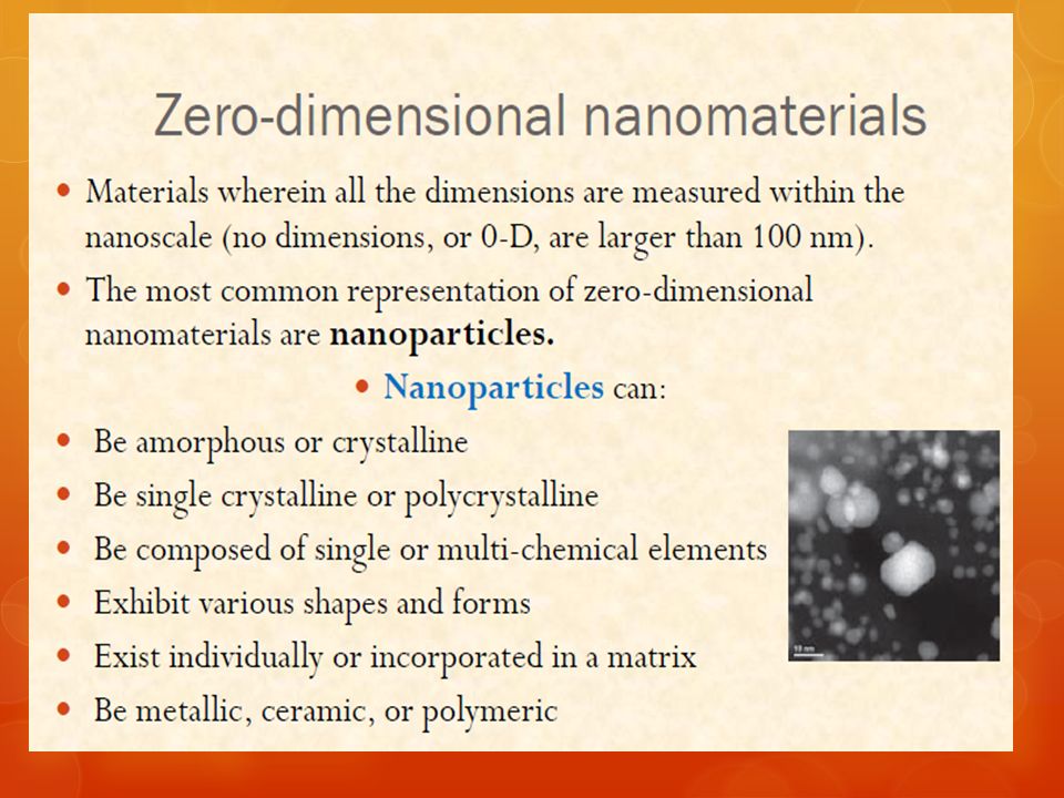
Nano Particles In nanotechnology, a particle is defined as a small object that behaves as a whole unit with respect to its transport and properties. Particles are further classified according to diameter. Coarse particles cover a range between 2,500 and 10,000 nanometers. Fine particles are sized between 100 and 2,500 nanometers. Ultrafine particles, or nanoparticles, are between 1 and 100 nanometers in size.nanotechnology Particlesnanometers

15
QUANTUM DOTS semiconductor nanoparticles are called Quantum dots- where excitons are confined in all the three directions and have properties combained between bulk and those of atoms

16
Nanorings A nanoring is a small ringformed crystal. The first nanoring made was a zinc oxide nanoring discovered by researchers at Georgia Institute of Technology. They are made by a spontaneous self-coiling process of nanobelts. Many layers of nanobelts are rolled together as coils, layer-by- layer.zinc oxideGeorgia Institute of Technology nanobelts

17
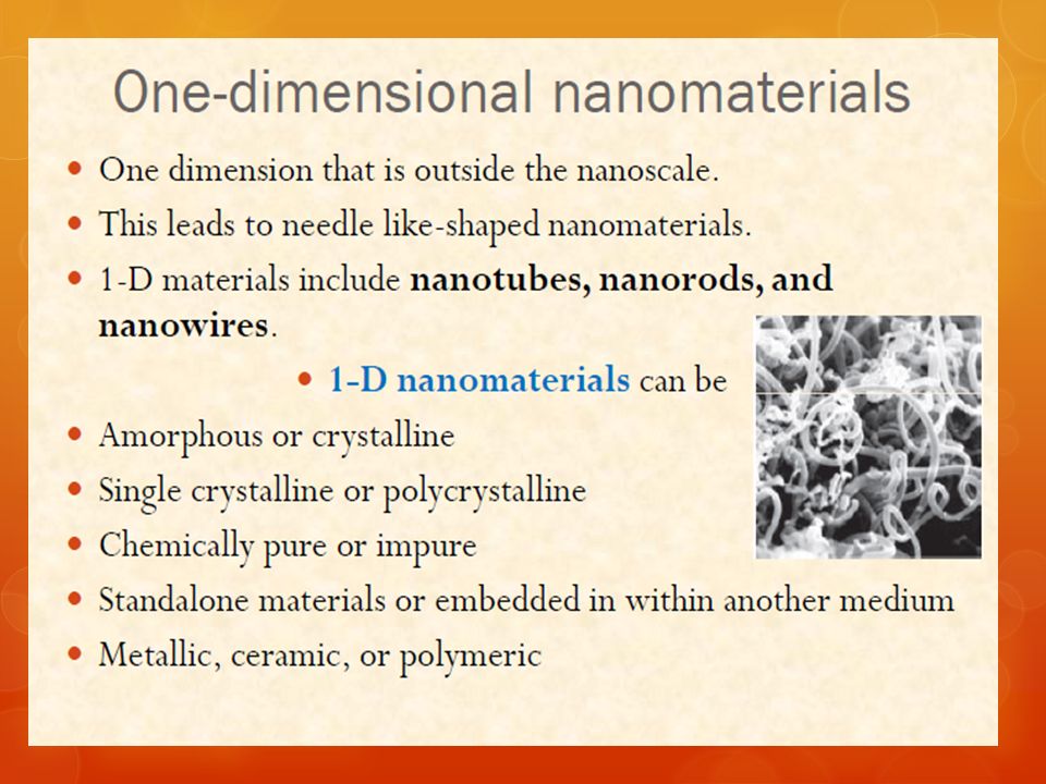
Nano wires A nanowire is a wire of dimension of the order of nanometres

18
Nanorods In nanotechnology, nanorods are one morphology of nanoscale objects. Each of their dimensions range from 1–100 nm. They may be synthesized from metals or semiconducting materials. Standard aspect ratios (length divided by width) are 3-5. Nanorods are produced by direct chemical synthesis. A combination of ligands act as shape control agents and bond to different facets of the nanorod with different strengths. This allows different faces of the nanorod to grow at different rates, producing an elongated object.nanotechnologynmaspect ratios chemical synthesis ligands
 are 3-5. Nanorods are produced by direct chemical synthesis. A combination of ligands act as shape control agents and bond to different facets of the nanorod with different strengths. This allows different faces of the nanorod to grow at different rates, producing an elongated object.nanotechnologynmaspect ratios chemical synthesis ligands.")
19
Nano -shells Nanoshells are nanoparticles that consist of an inner core of one type of material and an outer layer of another only a few nanometers thick. One application of nanotechnology in biomedicine is to create nanoshells that absorb at biologically useful wavelengths, depending on the shell thickness.nanotechnology

21
In this group of composites the main part of the volume is occupied by a ceramic, i.e. a chemical compound from the group of oxides, nitrides, borides, silicides etc.. In most cases, ceramic-matrix nanocomposites encompass a metal as the second component. Ideally both components, the metallic one and the ceramic one, are finely dispersed in each other in order to elicit the particular nanoscopic properties.ceramicmetal Ceramic-matrix nanocomposites Metal-matrix nanocomposites Metal matrix nanocomposites can also be defined as reinforced metal matrix composites. This type of composites can be classified as continuous and non- continuous reinforced materials. One of the more important nanocomposites is Carbon nanotube metal matrix composites, which is an emerging new material that is being developed to take advantage of the high tensile strength and electrical conductivity of carbon nanotube materials. Carbon nanotube metal matrix composites Polymer-matrix nanocomposites In the simplest case, appropriately adding nanoparticulates to a polymer matrix can enhance its performance, often dramatically, by simply capitalizing on the nature and properties of the nanoscale filler ]. (these materials are better described by the term nanofilled polymer composites ). This strategy is particularly effective in yielding high performance composites, when good dispersion of the filler is achieved and the properties of the nanoscale filler are substantially different or better than those of the matrix.nanoparticulates
. This strategy is particularly effective in yielding high performance composites, when good dispersion of the filler is achieved and the properties of the nanoscale filler are substantially different or better than those of the matrix.nanoparticulates.")
22
Nano material classification OrganicFullerene(C60) Carbon nanotubes(CNT) In organic DNA The requirement of fast growing world cannot meet these Nano materials, so new class of materials are introduced known as Nano composites –materials derived the combination of two or more building blocks containing atleast one component in nanometer scale
 Carbon nanotubes(CNT) In organic DNA The requirement of fast growing world cannot meet these Nano materials, so new class of materials are introduced known as Nano composites –materials derived the combination of two or more building blocks containing atleast one component in nanometer scale")
23
Carbon based nanomaterials Fullerene Compsed of stacked graphene sheets of linked hexagonal rings/ pentagonal rings as the basis of a closed cage structure They are spherical or ellipsoidal shapes. Spherical fullerenes are called Bucky balls Carbon nanotubes There can be single walled or multiwalled CNTs obtained by wrapping one atom thick layer of graphite into continuous smooth cylinder. They are cylindrical nanostructures with aspect ratio (length to diameter) of the order of 10 8 and are called Bucky tubes
 of the order of 10 8 and are called Bucky tubes.")
24
Fullerene Fullerene, a molecule composed of carbon atoms that form a hollow, cage like structure. The arrangement of the atoms produces pentagonal and hexagonal shapes— that is, shapes with five or six sides, C60C70

25
Carbon nanotube Carbon nanotubes (CNTs) are allotropes of carbon with a cylindrical nanostructure. Nanotubes have been constructed with length-to-diameter ratio of up to 132,000,000:1, significantly larger than for any other material. These cylindrical carbon molecules have unusual properties, which are valuable for nanotechnology, electronics, optics and other fields of materials science and technologyallotropes of carboncylindrical nanostructurecarbonmoleculesnanotechnologyelectronicsopticsmaterials science

26
Dendrimers These are nano sized polymers builtfrom branched unitsIts surface has numerous chain ends which can be tailored to perform specific chemical functions

28
PROPERTIES OF NANOMATERIALS 1. Optical properties 2. Electrical properties 3. Chemical properties 4. Physical prperties 5. Mechanical properties 6. Magnetic properties

29
Optical properties At nanocsale level physical properties become size dependent. Colour and transparency are obseved to change at nanoscale -nanoparticles are so small that electrons in them are not as much free to move as in the bulk material, due to this nanoparticles react differently with light

30
Electrical properties The ionization potential at small sizes are higher than that of the bulk. The ionization potential show marked fluctuation as function of size The change in electrical properties in nanomatrials can not be generalized The current –voltage characteristics (I-V ) of nanoparticles is a staircase type In nanoceramics and magnetic nanocomposites, the electrical conductivity increases with reduction in particle size, while in nanometals the electrical conductivity decreases with reduction particle size. In the case of carbon nanotubes the conductivity changes with change in diameter, it also changes with twist applied to the nanotubes
 of nanoparticles is a staircase type In nanoceramics and magnetic nanocomposites, the electrical conductivity increases with reduction in particle size, while in nanometals the electrical conductivity decreases with reduction particle size. In the case of carbon nanotubes the conductivity changes with change in diameter, it also changes with twist applied to the nanotubes.")
31
Chemical properties Since the percentage of surface atoms is large in the nanoparticles as compared with bulk materials, the reactivities of nanomaterials are more than the bulk materials

32
Physical properties Properties like strength, melting point eic. Change drasitcally at nanoscale At macro level steel is stronger than carbon, however at nanolevel the CNTs are found to be 100 times stronger than steel and it is more flexible too The melting point usually does not change with change in size at maroscopic level, however at nanoscale, if the size of the object is changed, then the percentage change in the no. of atoms on the surface is very large, the melting point start depending on the size of the object and goes on decreaseing with decrease in size

33
Mechanical properties In nanometre scale, the surface atoms face different potentials in different directions.The resulting stress modifies the mechanical and structural properties They become more hard and wear resistant The elastic properties like Youngs modulus decreases with decrease in size The fatigue strength increases with reduction in grain size of the materials - which finds application ins in the construction of air crafts They superelastic materials as they have extensive tensile deformation without cracking or fracture Energy dissipation, mechanical coupling within array of components and mechanical non-linearities are influenced by structuring components at the nm scale

34
Magnetic properties Magnetic Nanoparticles show unusual magnetic behaviour compared to the bulk materials Nanosized particles of magnetite show supermagnetism at transition tempertature which is smaller than the transition temp of the bulk

35
APPLICATIONS Nanomaterials posses unique and benificialchemical physical and mechanical properties, they can be used for a variety of applications 1.Cosmetics- eg. Sunscreen lotions, creams etc. 2.Nanocomposite materials 3.Nanocoatings 4.High performance paints 5.Next generation computer chips 6.Better insulating materials 7. High performance TV- use of nanophosphors render very high resolution low cost flat panel displays 8.Tougher and harder cutting tools

36
Applications– continue… 9. Elimination of pollutants 10.High power magnets 11.High sensitivity sensors 12. Automobiles with greater fuel efficiency 13. Better weapons 14. Long lasting medical implants 15. Ductile,machinable ceramics 16. In medicine- discease diagnosis, drug delivery etc. 17. In Biotechnology 18. Electromagnetic display devices

37
37 Thank You

Similar presentations


 –8 C atoms.>")
 Discovery and Applications of fullerenes.>")

>")


>")


