Download presentation
Presentation is loading. Please wait.

1
CORRECTION Last session, I have made a mistake about two digital coding methods. I explained Hamming code as Grey code mistakenly. Here is correct explanation of Grey code. 0000 0001 00100011 0010 01000110 01010111 01100101 01110100 10001100 10011101 10101111 10111110 11001010 11011011 11101001 1111000

2
COMBINATIONAL CIRCUITS LOGIC CIRCUITS: 1. Combinational 2. Sequential Combinational logic circuits (circuits without a memory): Combinational switching networks whose outputs depend only on the current inputs. Sequential logic circuits (circuits with memory): In this kind of network, the outputs depend on the current inputs and the previous inputs. These networks employ storage elements and logic gates. [Chapters 5 and 9]
: Combinational switching networks whose outputs depend only on the current inputs. Sequential logic circuits (circuits with memory): In this kind of network, the outputs depend on the current inputs and the previous inputs. These networks employ storage elements and logic gates. [Chapters 5 and 9].")
3
COMBINATIONAL CIRCUITS Most important standard combinational circuits are: Adders Subtractors Comparators Decoders Encoders Multiplexers Available in IC’s as MSI and used as standard cells in complex VLSI (ASIC)
")
4
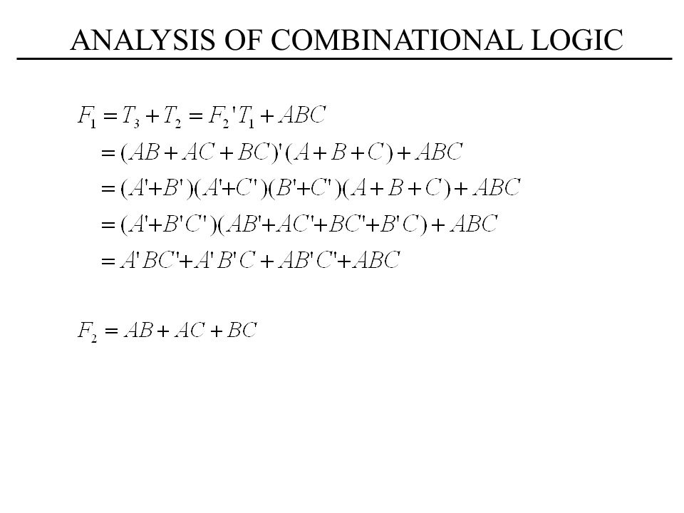
ANALYSIS OF COMBINATIONAL LOGIC

6
InputsOutputs ABCF1F1 F2F2 00000 00110 01010 01101 10010 10101 11001 11111 INPUTSOUTPUTS ANALYSIS OF COMBINATIONAL LOGIC From the truth table can you tell the function of the circuit?

7
//Example 4-10 //------------------------------------------ //Gate-level description of combinational circuit module analysis (A,B,C,F1,F2); input A,B,C; output F1,F2; wire T1,T2,T3,F2not,E1,E2,E3; or g1 (T1,A,B,C); and g2 (T2,A,B,C); and g3 (E1,A,B); and g4 (E2,A,C); and g5 (E3,B,C); or g6 (F2,E1,E2,E3); not g7 (F2not,F2); and g8 (T3,T1,F2not); or g9 (F1,T2,T3); endmodule COMBINATIONAL LOGIC - Verilog CODE
; input A,B,C; output F1,F2; wire T1,T2,T3,F2not,E1,E2,E3; or g1 (T1,A,B,C); and g2 (T2,A,B,C); and g3 (E1,A,B); and g4 (E2,A,C); and g5 (E3,B,C); or g6 (F2,E1,E2,E3); not g7 (F2not,F2); and g8 (T3,T1,F2not); or g9 (F1,T2,T3); endmodule COMBINATIONAL LOGIC - Verilog CODE")
8
COMBINATIONAL LOGIC - HDL CODE //Stimulus to analyze the circuit module test_circuit; reg [2:0]D; *input specified with a 3-bit reg vector D: 0 2 wire F1,F2; *outputs analysis circuit(D[2],D[1],D[0],F1,F2); *D[2]=A, D[1]=B, D[0]=C initial begin D = 3'b000; *D is a 3-bit vector initialized to 000 repeat(7) *The repeat loop gives the 7 binary numbers after 000 #10 D = D + 1'b1; *D is incremented by 1 after 10 ns end initial $monitor ("ABC = %b F1 = %b F2 =%b ",D, F1, F2); *Display truth table endmodule Simulation Log: ABC = 000 F1 = 0 F2 = 0 ABC = 001 F1 = 1 F2 = 0 ABC = 010 F1 = 1 F2 = 0
![COMBINATIONAL LOGIC - HDL CODE //Stimulus to analyze the circuit module test_circuit; reg [2:0]D; *input specified with a 3-bit reg vector D: 0 2 wire F1,F2; *outputs analysis circuit(D[2],D[1],D[0],F1,F2); *D[2]=A, D[1]=B, D[0]=C initial begin D = 3 b000; *D is a 3-bit vector initialized to 000 repeat(7) *The repeat loop gives the 7 binary numbers after 000 #10 D = D + 1 b1; *D is incremented by 1 after 10 ns end initial $monitor ( ABC = %b F1 = %b F2 =%b ,D, F1, F2); *Display truth table endmodule Simulation Log: ABC = 000 F1 = 0 F2 = 0 ABC = 001 F1 = 1 F2 = 0 ABC = 010 F1 = 1 F2 = 0](http://images.slideplayer.com/24/7023502/slides/slide_8.jpg "COMBINATIONAL LOGIC - HDL CODE //Stimulus to analyze the circuit module test_circuit; reg [2:0]D; *input specified with a 3-bit reg vector D: 0 2 wire F1,F2; *outputs analysis circuit(D[2],D[1],D[0],F1,F2); *D[2]=A, D[1]=B, D[0]=C initial begin D = 3 b000; *D is a 3-bit vector initialized to 000 repeat(7) *The repeat loop gives the 7 binary numbers after 000 #10 D = D + 1 b1; *D is incremented by 1 after 10 ns end initial $monitor ( ABC = %b F1 = %b F2 =%b ,D, F1, F2); *Display truth table endmodule Simulation Log: ABC = 000 F1 = 0 F2 = 0 ABC = 001 F1 = 1 F2 = 0 ABC = 010 F1 = 1 F2 = 0")
9
DESIGN OF COMBINATIONAL LOGIC 1.From the specifications of the circuit, determine the number of inputs and outputs 2.Derive the truth table that defines the relationship between the input and the output. 3.Obtain the simplified Boolean function using x-variable K-Map. 4.Draw the logic diagram and verify the correctness of the design.

10
DESIGN OF COMBINATIONAL LOGIC Example: Design a combinational circuit with three inputs and one output. The output is a 1 when the binary value is less than three. The output is 0 otherwise. xyzF 0001 0011 0101 0110 1000 1010 1100 1110 111 00 01 11 10 0 1 y x z y z

11
ARITHMETIC LOGIC UNIT (ALU) Copyright: Tylavsky, Arizona State University
 Copyright: Tylavsky, Arizona State University")
12
BINARY ADDER – Half Adder ABSC 0000 1010 0110 1101

13
InputsOutputs ABCF1F1 F2F2 00000 00110 01010 01101 10010 10101 11001 11111 INPUTSOUTPUTS BINARY ADDER - Full Adder C

14
Full Adder in SOP

15
Note mistake in Fig. 4-6: S should be C Implementation Full Adder with two half Adders

16
CASCADE 4-BIT FULL ADDER 0110CiCi 1011AiAi 0011BiBi 1110SiSi 0011C i+1 3210i

17
//Gate-level hierarchical description of 4-bit adder // Description of half adder (see Fig 4-5b) module halfadder (S,C,x,y); input x,y; output S,C; //Instantiate primitive gates xor (S,x,y); and (C,x,y); endmodule //Description of full adder (see Fig 4-8) module fulladder (S,C,x,y,z); input x,y,z; output S,C; wire S1,D1,D2; //Outputs of first XOR and two AND gates //Instantiate the halfadder halfadder HA1 (S1,D1,x,y), HA2 (S,D2,S1,z); or g1(C,D2,D1); endmodule CASCADE 4-BIT FULL ADDER - HDL CODE 1
 module halfadder (S,C,x,y); input x,y; output S,C; //Instantiate primitive gates xor (S,x,y); and (C,x,y); endmodule //Description of full adder (see Fig 4-8) module fulladder (S,C,x,y,z); input x,y,z; output S,C; wire S1,D1,D2; //Outputs of first XOR and two AND gates //Instantiate the halfadder halfadder HA1 (S1,D1,x,y), HA2 (S,D2,S1,z); or g1(C,D2,D1); endmodule CASCADE 4-BIT FULL ADDER - HDL CODE 1")
18
//Description of 4-bit adder (see Fig 4-9) module _4bit_adder (S,C4,A,B,C0); input [3:0] A,B; input C0; output [3:0] S; output C4; wire C1,C2,C3; //Intermediate carries //Instantiate the fulladder fulladder FA0 (S[0],C1,A[0],B[0],C0), FA1 (S[1],C2,A[1],B[1],C1), FA2 (S[2],C3,A[2],B[2],C2), FA3 (S[3],C4,A[3],B[3],C3); endmodule CASCADE 4-BIT FULL ADDER - HDL CODE 2
![//Description of 4-bit adder (see Fig 4-9) module _4bit_adder (S,C4,A,B,C0); input [3:0] A,B; input C0; output [3:0] S; output C4; wire C1,C2,C3; //Intermediate carries //Instantiate the fulladder fulladder FA0 (S[0],C1,A[0],B[0],C0), FA1 (S[1],C2,A[1],B[1],C1), FA2 (S[2],C3,A[2],B[2],C2), FA3 (S[3],C4,A[3],B[3],C3); endmodule CASCADE 4-BIT FULL ADDER - HDL CODE 2](http://images.slideplayer.com/24/7023502/slides/slide_18.jpg "//Description of 4-bit adder (see Fig 4-9) module _4bit_adder (S,C4,A,B,C0); input [3:0] A,B; input C0; output [3:0] S; output C4; wire C1,C2,C3; //Intermediate carries //Instantiate the fulladder fulladder FA0 (S[0],C1,A[0],B[0],C0), FA1 (S[1],C2,A[1],B[1],C1), FA2 (S[2],C3,A[2],B[2],C2), FA3 (S[3],C4,A[3],B[3],C3); endmodule CASCADE 4-BIT FULL ADDER - HDL CODE 2")
Similar presentations
; input.>")


>")
 Lecture-8:>")


;>")


