Download presentation
Presentation is loading. Please wait.

1
2. Transistors and Layout Fabrication techniques Transistors and wires Design rule for layout Basic concepts and tools for Layout

2
2.2 Fabrication Processes 2.2.1 Overview Minimum channel length=0.5μm λ=0.25μm ---- 0.5μProcess

3
2.2.2 Fabrication Steps Photoresist: mask pattern SiO 2 pattern Features are patterned on the wafer by a photolithographic process; The wafer is covered by light sensitive material “photoresist”. It is exposed to light with proper mask pattern. The patterns left by the photoresist can be used to control where SiO 2 is grown on materials.

4
1)Put tubs into wafer. 2)Form an oxide covering on wafer and the polysilicon wires. 3)Diffusion (wires) (polysilicon masks the formation of diffusion wires.=self- aligned) 4)Metal connections are made with filling cuts (via) to make connections after another oxide layer is deposited. Steps in processing a wafer (twin tub process)
Diffusion (wires) (polysilicon masks the formation of diffusion wires.=self- aligned) 4)Metal connections are made with filling cuts (via) to make connections after another oxide layer is deposited. Steps in processing a wafer (twin tub process).")
5
“MOS” : sandwich of Metal, Oxide, and Silicon (semiconductor substrate). The positive voltage on the polysilicon forms gate attracts the elctoron at the top of the channel. The threshold voltage (Vt) collects enough electrons at the channel boundary to form an inversion layer (p -> n). 2.3 Transistors 2.3.1 Structures of Transistors Gate Oxide Field Oxide
 collects enough electrons at the channel boundary to form an inversion layer (p -> n). 2.3 Transistors Structures of Transistors Gate Oxide Field Oxide.")
7
Layout of n-type and p-type transistors nMOS pMOS nMOS with wide width

8
Linear region Saturated region 2.3.2 A Simple Transistor Model

9
Cg: gate capacitance = 0.9fF/μm 2 (2 μprocess) Cgs/Cgd: source/drain overlap capacitance =Cox W (Cox: gate/bulk overlap capacitance) 2.3.3 Transistor Parasitics
 Cgs/Cgd: source/drain overlap capacitance =Cox W (Cox: gate/bulk overlap capacitance) Transistor Parasitics")
10
Tub Ties (substrate bias) 2.2.4 Tub Layout and Latchup
 Tub Layout and Latchup")
11
Tubo Layout and Latchup

12
2.2.5 Advanced Transistor Characteristics Parallel plate oxide capacitance per unit area Cox = ε ox /x ox where ε ox = permittivity of silicon dioxide = (3.9 ε o ) x ox = oxide thickness
 x ox = oxide thickness")
13
Q(y)=Cox(Vgs-Vt-Vy) dV=Iydy/μQ(y)W Shape of the inversion layer as a function of gate voltage
=Cox(Vgs-Vt-Vy) dV=Iydy/μQ(y)W Shape of the inversion layer as a function of gate voltage")
15
Wires of different layers are insulated by an additional layer of SiO 2. Vias are cuts in the insulating SiO 2. 2.4 Wires and Vias

16
The mean time for failure (MTF) MTF=j -n e (Q/kT). j:current density n:constant(1~2) Q:diffusion activation energy. j Metal < 1.5mA/μm width (4.5mA by 3μm width wire) MTF for metal wires
 Q:diffusion activation energy. j Metal < 1.5mA/μm width (4.5mA by 3μm width wire) MTF for metal wires.")
17
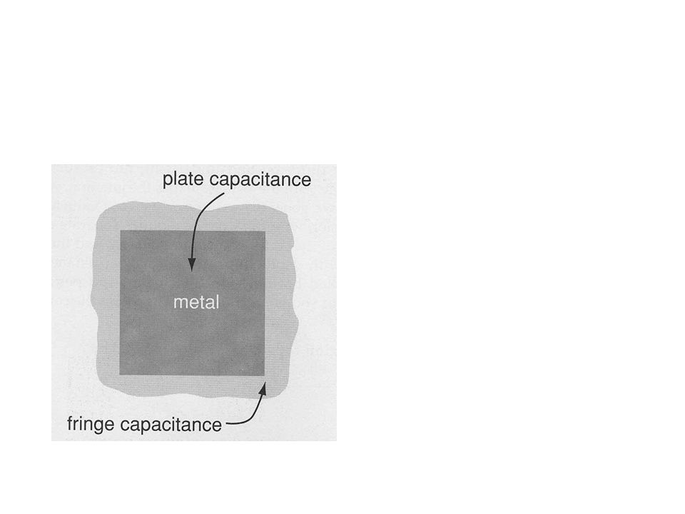
C j0 = ε Si /x d Depletion region capacitance C j0 : zero-bias depletion capacitance ε Si : permittivity of silicon x d : thickness of depletion region depending on applied voltage. 2.4.1 Wire Parasitics

19
0.3fF/cm 2 (overlapping area) 0.1fF/cm 2 metal 3 Depending on distance
 0.1fF/cm 2 metal 3 Depending on distance")
20
0.5 μm process (λ=0.25 μm) 1) Unit bottomwall capacitance C1_0=0.6fF/μm 2 Area=3 μm x 0.75 μm+1.0 μm x 1.0 μm=3.25 μm 2 (3.25 λ 2 μm 2 ) C1=0.6fF(/ λ 2 ) x 3.25 (xλ 2 )=1.95 fF 2 ) Unit sidewall capacitance C2_0=0.2fF/μm Perimeter=0.75+4+1+1+0.25+3=10 μm C2=0.2fFx10=2fF 3) Metal capacitance C3_0=0.04fF/ μm 2 Area=2.5 μm x 1.5 μm=3.75μm 2 C3=0.04fFx3.75=0.15fF 4) Metal fringe capacitance C4_0=0.09fF /μm Perimeter=(2.5+1.5)x2=8 μm C4=0.09fFx8=0.72fF 5) Total capacitance=1.95+2+0.15+0.72=4.85fF Example of Parasitic capacitance measurement
 1) Unit bottomwall capacitance C1_0=0.6fF/μm 2 Area=3 μm x 0.75 μm+1.0 μm x 1.0 μm=3.25 μm 2 (3.25 λ 2 μm 2 ) C1=0.6fF(/ λ 2 ) x 3.25 (xλ 2 )=1.95 fF 2 ) Unit sidewall capacitance C2_0=0.2fF/μm Perimeter= =10 μm C2=0.2fFx10=2fF 3) Metal capacitance C3_0=0.04fF/ μm 2 Area=2.5 μm x 1.5 μm=3.75μm 2 C3=0.04fFx3.75=0.15fF 4) Metal fringe capacitance C4_0=0.09fF /μm Perimeter=( )x2=8 μm C4=0.09fFx8=0.72fF 5) Total capacitance= =4.85fF Example of Parasitic capacitance measurement")
21
Ohms per square [Ω/ ] = Sheet resistance Example of Resistance Measurement 0.5 μm process (λ=0.25 μm) 1)Polysilicon resistance Rpoly=[18/3]x4[ Ω/ ]=24 Ω 2)n-diffusion resistance [(9/3)+(6/3)+1/2]x 2 [Ω/ ] =11 Ω
![Ohms per square [Ω/ ] = Sheet resistance Example of Resistance Measurement 0.5 μm process (λ=0.25 μm) 1)Polysilicon resistance Rpoly=[18/3]x4[ Ω/ ]=24 Ω 2)n-diffusion resistance [(9/3)+(6/3)+1/2]x 2 [Ω/ ] =11 Ω](http://images.slideplayer.com/24/6927104/slides/slide_21.jpg "Ohms per square [Ω/ ] = Sheet resistance Example of Resistance Measurement 0.5 μm process (λ=0.25 μm) 1)Polysilicon resistance Rpoly=[18/3]x4[ Ω/ ]=24 Ω 2)n-diffusion resistance [(9/3)+(6/3)+1/2]x 2 [Ω/ ] =11 Ω")
22
Problems when wire are too wide or narrow. Polysilicon should extend beyond boundary of difusion area. The cut of via must connect elements and not mistakenly connect to substrate or others. 2.5 Design Rule 2.5.1 Fabrication Errors

23
All physical parameters to be shrunk by a factor 1/x Lengths: W–› W/x Widths:L –› L/x Vertical dimensions such as oxide thickness: t ox –› t ox /x Doping concentrations: N d –› N d /x Supply voltages: V DD -V SS –› (V DD -V SS ) Id’/Id =1/x Cg’/Cg =1/x (C’V’/I’)/(CV/I) = 1/x 2.5.2 Scalable Design Rules
 Id’/Id =1/x Cg’/Cg =1/x (C’V’/I’)/(CV/I) = 1/x Scalable Design Rules")
24
Metal1 min-width=3λ, min-sep= 3λ Metal2 min-width=3λ, min-sep= 3λ poly min-width=2λ, min-sep= 2λ n, p-dif min-width=3λ, min-sep(n-n, p-p)= 3λ (n-p 10λ) Tube min-width=10λ, min-distance(tub- active)= 5λ Transistors min-W/L=3λ/2λ poly extension= 2λ dif extension= 2λ active-poly/metal via=λ min-sep(tran.-tran.)= 2λ min-sep(tran-tub.tie) = 3λ 2.5.2 SCMOS Design Rules
= 3λ (n-p 10λ) Tube min-width=10λ, min-distance(tub- active)= 5λ Transistors min-W/L=3λ/2λ poly extension= 2λ dif extension= 2λ active-poly/metal via=λ min-sep(tran.-tran.)= 2λ min-sep(tran-tub.tie) = 3λ SCMOS Design Rules")
25
Vias cuts=2λx2λ via =4λx4λ n,p.diff-poly, poly-metal1 n,p.diff-metal1, metal1-metal2 Tub ties cuts =2λx2λ metal =4λx4λ Metal1 min-width=6λ, min-sep= 4λ available via to metal2 Special rules cut to poly – poly sep =3 λ poly.cut-dif.cut sep=2λ cut-tran.active sep =2λ dif.cut-dif sep = 4λ meta2.via must not be directly over polysilicon Prohibit small negative features. SCMOS Design Rules (continue)
.")
26
2.5.4 Typical Process Parameters

27
Net: a set of electrical connections Wire: a set of point-point connections. Wire segment: a straight section of wire. Circuit schematic: n-type, p-type transistors with W/L 2.6 Layout Design and Tools 2.6.1 Layouts for Circuits

28
Design of an inverter layout

29
2.6.2 Stick Diagram

30
Rules for possible interaction between layers

31
2.6.3 Hierarchical Stick Diagrams

32
Example of stick design of a multiplexer

33
Example of stick design of a multiplexer (continue)
")
34
Layout Editors: intensive graphic program for manual layout symbolic layouts: more detail than stick diagram Design Rule Checkers (DRC): check items: minimum spacing minimum size combination of layers Circuit Extractions: extension of DRC (identify transistors and vias) a complete job of compnents and wire extraction to produce a net list from layout. 2.6.4 Layout Design and Analysis Tools

35
Basic Operation of Circuit Extraction NOT, AND, OR between 2 masks grow and shrink operation over masks. 1) extraction of transistors AND(poly - p/n.diff) 2) identify via grow cut AND( grown-cut, metal, poly ) Circuit Extraction
 extraction of transistors AND(poly - p/n.diff) 2) identify via grow cut AND( grown-cut, metal, poly ) Circuit Extraction.")
36
Flattening is required to make extracted netlist small by making correspondence between net names in cells and nets int the top-level components. Hierarchical Circuit Extraction

37
2.6.5 Automatic Layout Cell generator (or macrocell generator) parameterized layout
 parameterized layout")
38
Standard Cell Placement and Routing Logic gates, latches, flip-flops, or larger logic Routing channels

39
An Example of Standard Cell Layout 2 stages placement routing

Similar presentations


>")


