Download presentation
Presentation is loading. Please wait.

1
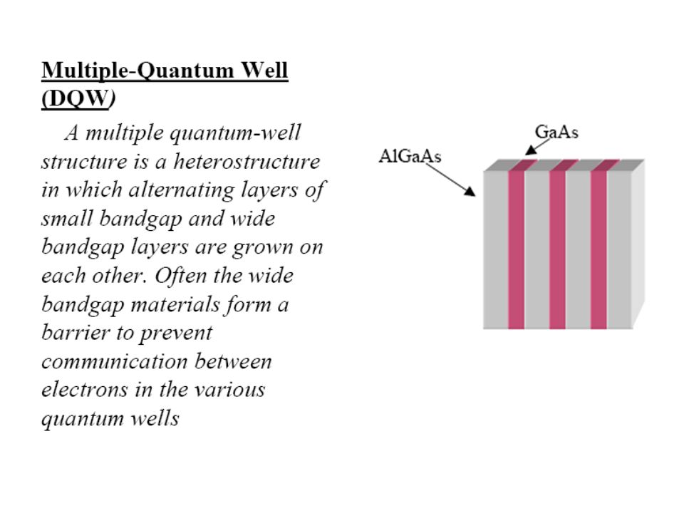
Unit-IV Nano Technology

4
SIZE A meter is about the distance from the tip of your nose to the end of your hand (1 meter = 3.28 feet). Millimeter- One thousandth of meter.(10-3m) Micron: a micron is a millionth of a meter (or) one thousandth of millimeter (10-6m) Nanometer: A nanometer is one thousandth of a micron (10–9m) (or) a billionth of a meter. ie.,one billion nanometers in a meter.
 Micron: a micron is a millionth of a meter (or) one thousandth of millimeter (10-6m) Nanometer: A nanometer is one thousandth of a micron (10–9m) (or) a billionth of a meter. ie.,one billion nanometers in a meter.")
6
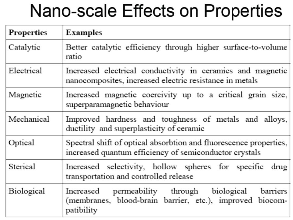
Composites made from particles of nano-size ceramics or metals smaller than 100 nanometers can suddenly become much stronger than predicted by existing materials-science models. For example, metals with a so-called grain size of around 10 nanometers are as much as seven times harder and tougher than their ordinary counterparts with grain sizes in the micro meter range. The Nano particles affects many properties such as Melting point Boiling point Band gap Optical properties Electrical properties Magnetic properties .Even the structure of materials changes with respect to Size

7
Nanoscale materials are divided into three category,
The properties of materials can be different at the Nanoscale for two main reasons: First, Nanomaterials have a relatively larger surface area when compared to the same mass of material produced in a larger form. Nano particles can make materials more chemically reactive and affect their strength or electrical properties. Second, quantum effects can begin to dominate the behaviour of matter at the Nanoscale Nanoscale materials are divided into three category, Zero dimension – length , breadth and heights are confined at single point. (for example, Nano dots) One dimension – It has only one parameter either length (or) breadth (or) height ( example:very thin surface coatings) Two dimensions- it has only length and breadth (for example, nanowires and nanotubes) Three dimensions -it has all parameter of length, breadth and height. (for example, Nano Particles).
 One dimension – It has only one parameter either length (or) breadth (or) height ( example:very thin surface coatings) Two dimensions- it has only length and breadth (for example, nanowires and nanotubes) Three dimensions -it has all parameter of length, breadth and height. (for example, Nano Particles).")
8
What do you mean by Nano Particles ?
Nano Particles are the particles of size between 1 nm to 100 nm 1 nm is only three to five atoms wide. ~40,000 times smaller than the width of an average human hair Nanometer - One billionth (10-9) of a meter • The size of Hydrogen atom 0.04 nm The size of Proteins ~ 1-20 nm Feature size of computer chips 180 nm Diameter of human hair ~ 10 µm At the nanoscale, the physical, chemical, and biological properties of materials differ in fundamental and valuable ways from the properties of individual atoms and molecules or bulk matter
 of a meter. • The size of Hydrogen atom 0.04 nm. The size of Proteins ~ 1-20 nm. Feature size of computer chips 180 nm. Diameter of human hair ~ 10 µm. At the nanoscale, the physical, chemical, and biological properties of materials differ in fundamental and valuable ways from the properties of individual atoms and molecules or bulk matter.")
9
Why Nano Particles ? Noparticles are of interest because of the new properties (such as chemical reactivity and optical behaviour) that they exhibit compared with larger particles of the same materials. For example, titanium dioxide and zinc oxide become transparent at the nanoscale and have found application in sunscreens. Nanoparticles have a range of potential applications: In the short-term application such as in cosmetics, textiles and paints. In the longer term applications such as drug delivery where they could be to used deliver drugs to a specific site in the body. Nanoparticles can also be arranged into layers on surfaces, providing a large surface area and hence enhanced activity, relevant to a range of potential applications such as catalysts.
 that they exhibit compared with larger particles of the same materials. For example, titanium dioxide and zinc oxide become transparent at the nanoscale and have found application in sunscreens. Nanoparticles have a range of potential applications: In the short-term application such as in cosmetics, textiles and paints. In the longer term applications such as drug delivery where they could be to used deliver drugs to a specific site in the body. Nanoparticles can also be arranged into layers on surfaces, providing a large surface area and hence enhanced activity, relevant to a range of potential applications such as catalysts.")
10
- Single electron transistors
• Examples - Carbon Nanotubes - Proteins, DNA - Single electron transistors AFM Image of DNA Carbon Nanotubes

11
Nanotechnology deals with the creation of USEFUL materials, devices and systems using the particles of nanometer length scale and exploitation of NOVEL properties (physical, chemical, biological) at that length scale
 at that length scale")
12
Various Nanomaterials and
Nanotechnologies Based on the size and shape, the Nano materials are classified as follows • Nanotubes • Nanosprings • Nanobelts • Quantum dots • Nanofluidies • Nanoparticles • Nanocapsules • Nanofibers • Nanowires • Fullerenes (carbon 60)
")
13
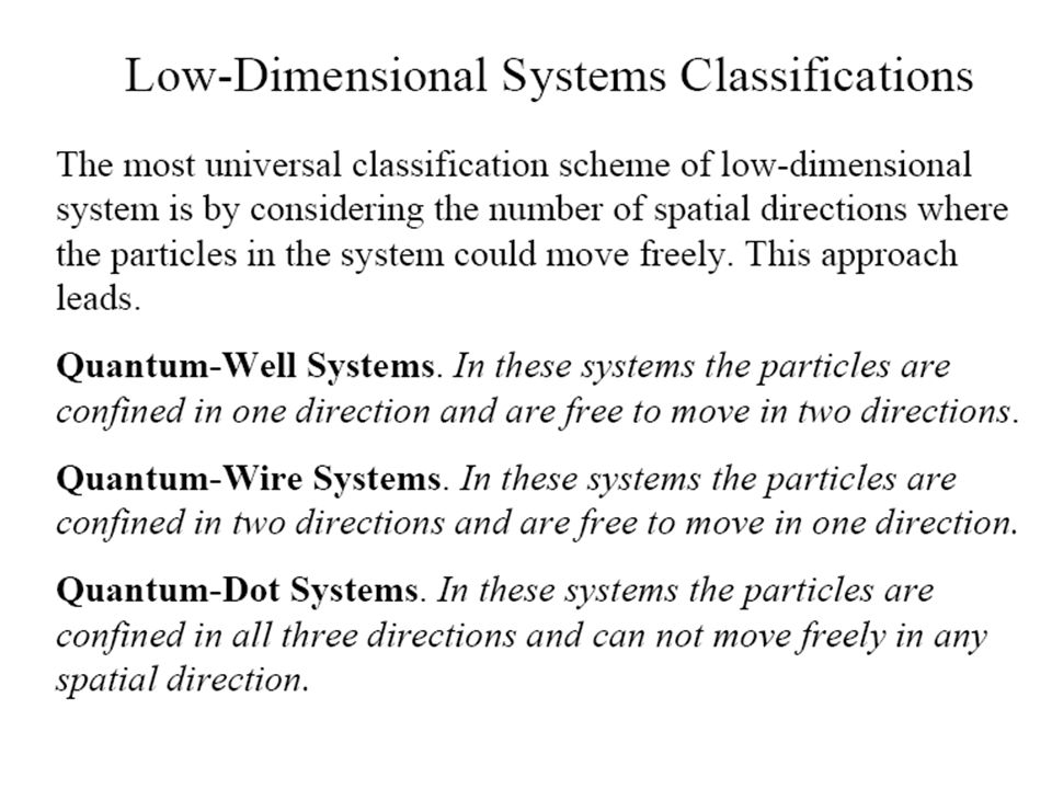
Quantum well Quantum Wire It is a two dimensional system
The electron can move in two directions and restricted in one direction. Quantum Wire It is a one-dimensional system The electron can move in one direction and restricted in two directions. Quantum dot It is a zero dimensional system The electron movement was restricted in entire three dimensions

14
Why called Quantum ? Because, the electronic property is quantized
The spatial distance is very very small

15
Semiconductor growth (single layer)
substrate Semiconductor growth (single layer)
")
18
Quantum wire Quantum wires are ultra fine wires or linear arrays of Nano dots, formed by self-assembly They can be made from a wide range of materials such as Semiconductor Nanowires made of silicon, gallium nitride and indium phosphide. Nanowires have potential applications in In high-density data storage, either as magnetic read heads or as patterned storage media In electronic and opto-electronic Nanodevices, for metallic interconnects of quantum devices and Nanodevices. Nanowires can be prepared by growth techniques such as Chemical Vapour deposition (CVD) Electroplating
 Electroplating.")
19
Quantum wire cont… In quantum wire, Two dimensions are reduced and one dimension remains large Therefore, the electrical resistivity of quantum wire can be calculated using conventional formula as follows, We need two dimension to calculate area of conducting material, but not present in quantum wire

20
General properties of Nanowire
Diameter – 10s of nanometers Single crystal formation -- common crystallographic orientation along the nanowire axis Minimal defects within wire Minimal irregularities within nanowire arrays Some example of Nanowire

21
Magnetic nanowires Example: Cobalt, gold, copper and cobalt-copper nanowire arrays Important for storage device applications Electrochemical deposition is the fabrication technique <20 nm diameter nanowire arrays can be fabricated by electrochemical deposition Cobalt nanowires on Si substrate (UMass Amherst, 2000)
")
22
In quantum dot all the three dimensions are reduced to zero

23
Dimension Variation

24
Properties of Nano Materials

26
Melting Point The melting point decreases dramatically as the particle size gets below 5 nm Source: Nanoscale Materials in Chemistry, Wiley, 2001

27
Band gap The band gap is increases with reducing the size of the particles

28
Surface Area The total surface area (or) the number of surface atom increases with reducing size of the particles
 the number of surface atom increases with reducing size of the particles.")
29
Properties of semiconductor and magnetic materials
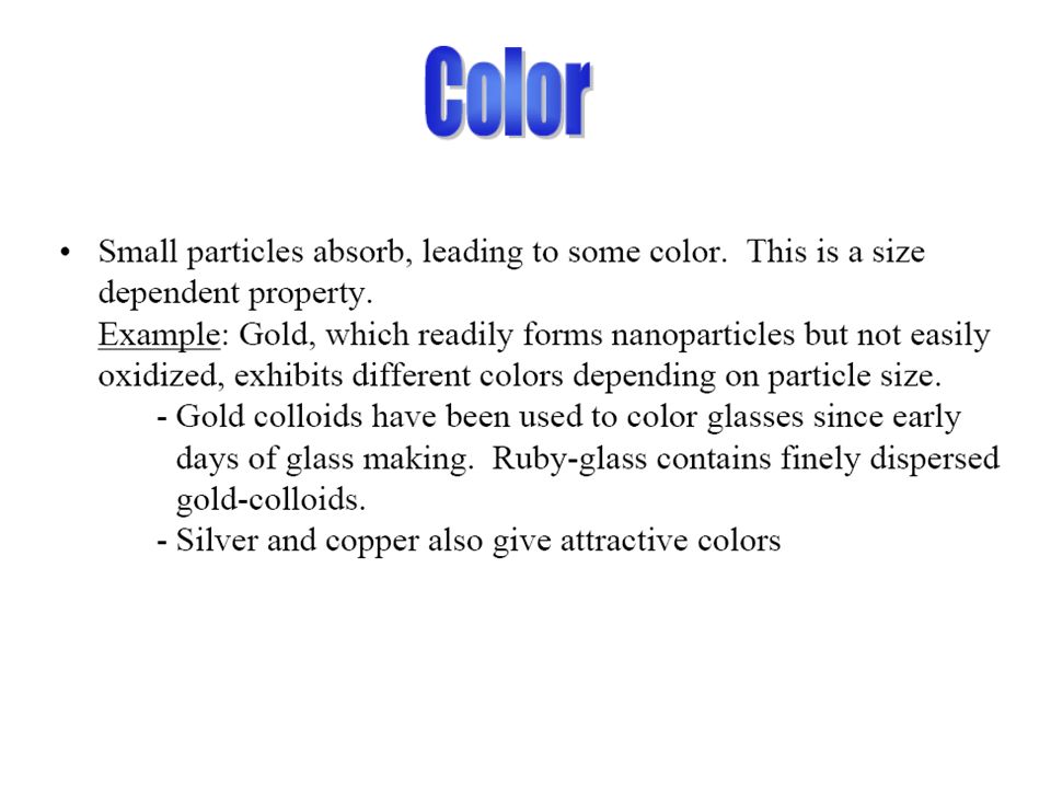
Size-Dependent Properties of semiconductor and magnetic materials • For semiconductors such as ZnO, CdS, and Si, the bandgap changes with size - Bandgap is the energy needed to promote an electron from the valence band to the conduction band - When the bandgaps lie in the visible spectrum, changing bandgap with size means a change in color • For magnetic materials such as Fe, Co, Ni, Fe3O4, etc., magnetic properties are size dependent - The ‘coercive force’ (or magnetic memory) needed to reverse an internal magnetic field within the particle is size dependent - The strength of a particle’s internal magnetic field can be size dependent
 needed to reverse an internal magnetic field within the particle is size dependent. - The strength of a particle’s internal magnetic field can be size dependent.")
31
Applications of Nano Materials

32
1. Nanotechnology Applications in Medicine
Because of their small size, nanoscale devices can readily interact with biomolecules on both the surface of cells and inside of cells. By gaining access to so many areas of the body, they have the potential to detect disease and the deliver treatment. Nanoparticles can can deliver drugs directly to diseased cells in your body. Nanomedicine is the medical use of molecular- sized particles to deliver drugs, heat, light or other substances to specific cells in the human body.

33
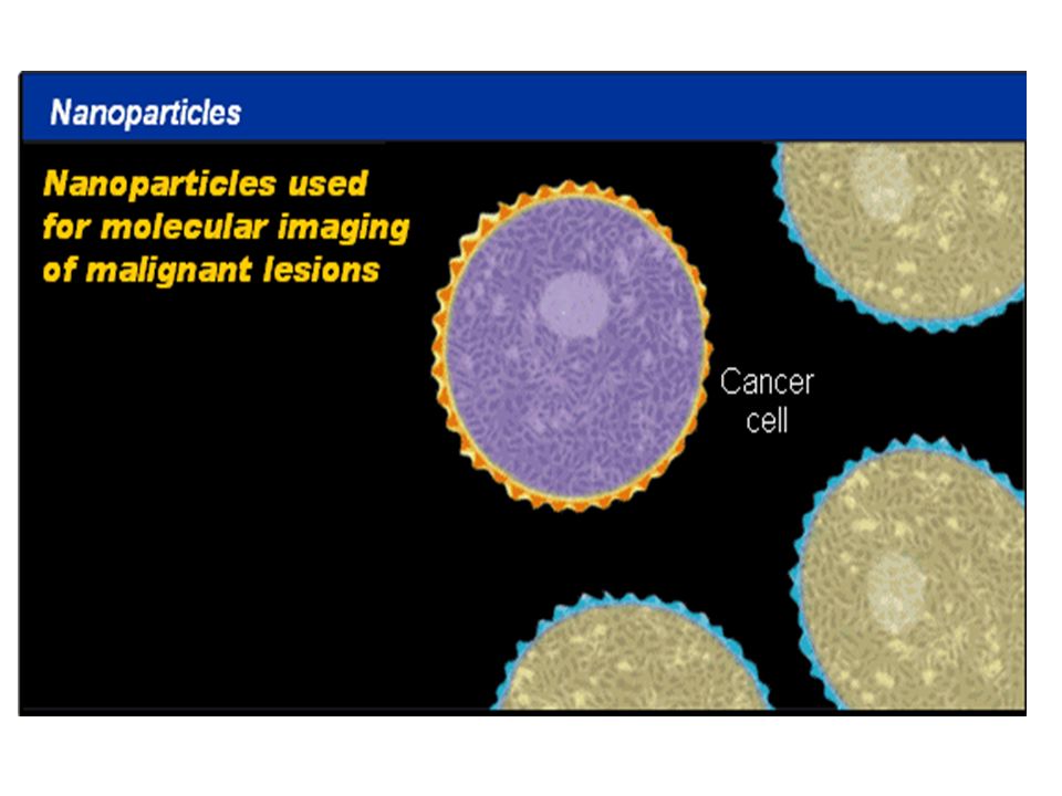
Quantum dot- that identify the location of cancer cells in the body.
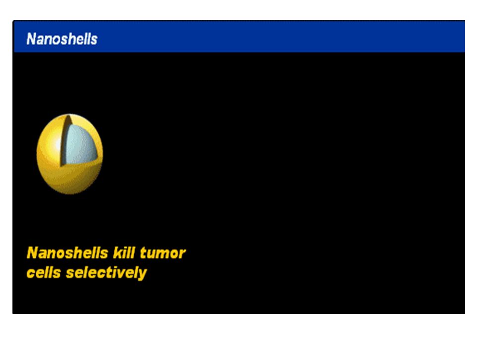
Nano Particles - that deliver chemotherapy drugs directly to cancer cells to minimize damage to healthy cells. Nanoshells - that concentrate the heat from infrared light to destroy cancer cells with minimal damage to surrounding healthy cells. Nanotubes- used in broken bones to provide a structure for new bone material to grow.

34
Nano shells as Cancer Therapy
Nano shells are injected into cancer area and they recognize cancer cells. Then by applying near-infrared light, the heat generated by the light-absorbing Nano shells has successfully killed tumor cells while leaving neighboring cells intact.

37
Nanowires – used as medical sensor
In this diagram (next page), Nano sized sensing wires are laid down across a micro fluidic channel. As particles flow through the micro fluidic channel, the Nanowire sensors pick up the molecular identifications of these particles and can immediately relay this information through a connection of electrodes to the outside world. These Nanodevices are man-made constructs made with carbon, silicon Nanowire. They can detect the presence of altered genes associated with cancer and may help researchers pinpoint the exact location of those changes
, Nano sized sensing wires are laid down across a micro fluidic channel. As particles flow through the micro fluidic channel, the Nanowire sensors pick up the molecular identifications of these particles and can immediately relay this information through a connection of electrodes to the outside world. These Nanodevices are man-made constructs made with carbon, silicon Nanowire. They can detect the presence of altered genes associated with cancer and may help researchers pinpoint the exact location of those changes.")
39
2. Nano Computing Technology
Past Shared computing thousands of people sharing a mainframe computer Present Personal computing Future Ubiquitous computing thousands of computers sharing each and everyone of us; computers embedded in walls, chairs, clothing, light switches, cars….; characterized by the connection of things in the world with computation.

40
3. Sunscreens and Cosmetics
Nanosized titanium dioxide and zinc oxide are currently used in some sunscreens, as they absorb and reflect ultraviolet (UV) rays. Nanosized iron oxide is present in some lipsticks as a pigment. Fuel Cells The potential use of nano-engineered membranes to intensify catalytic processes could enable higher-efficiency, small-scale fuel cells. Displays Nanocrystalline zinc selenide, zinc sulphide, cadmium sulphide and lead telluride are candidates for the next generation of light-emitting phosphors. CNTs are being investigated for low voltage field-emission displays; their strength, sharpness, conductivity and inertness make them potentially very efficient and long-lasting emitters.
 rays. Nanosized iron oxide is present in some lipsticks as a pigment. 4. Fuel Cells. The potential use of nano-engineered membranes to intensify catalytic processes could enable higher-efficiency, small-scale fuel cells. 5. Displays. Nanocrystalline zinc selenide, zinc sulphide, cadmium sulphide and lead telluride are candidates for the next generation of light-emitting phosphors. CNTs are being investigated for low voltage field-emission displays; their strength, sharpness, conductivity and inertness make them potentially very efficient and long-lasting emitters.")
41
6. Batteries With the growth in portable electronic equipment (mobile phones, navigation devices, laptop computers, remote sensors), there is great demand for lightweight, high-energy density batteries. Nanocrystalline materials are candidates for separator plates in batteries because of their foam-like (aerogel) structure, which can hold considerably more energy than conventional ones. Nickel–metal hydride batteries made of nanocrystalline nickel and metal hydrides are envisioned to require less frequent recharging and to last longer because of their large grain boundary (surface) area. 7. Catalysts In general, nanoparticles have a high surface area, and hence provide higher catalytic activity.
, there is great demand for lightweight, high-energy density batteries. Nanocrystalline materials are candidates for separator plates in batteries because of their foam-like (aerogel) structure, which can hold considerably more energy than conventional ones. Nickel–metal hydride batteries made of nanocrystalline nickel and metal hydrides are envisioned to require less frequent recharging and to last longer because of their large grain boundary (surface) area. 7. Catalysts. In general, nanoparticles have a high surface area, and hence provide higher catalytic activity.")
42
8. Magnetic Nano Materials applications
It has been shown that magnets made of nanocrystalline yttrium–samarium–cobalt grains possess unusual magnetic properties due to their extremely large grain interface area (high coercivity can be obtained because magnetization flips cannot easily propagate past the grain boundaries). This could lead to applications in motors, analytical instruments like magnetic resonance imaging (MRI), used widely in hospitals, and microsensors. Nanoscale-fabricated magnetic materials also have applications in data storage. Devices such as computer hard disks storage capacity is increased with Magnetic Nano materials
. This could lead to applications in motors, analytical instruments like magnetic resonance imaging (MRI), used widely in hospitals, and microsensors. Nanoscale-fabricated magnetic materials also have applications in data storage. Devices such as computer hard disks storage capacity is increased with Magnetic Nano materials.")
43
9. Medical Implantation Unfortunately, in some cases, the biomedical metal alloys may wear out within the lifetime of the patient. But Nano materials increases the life time of the implant materials. Nanocrystalline zirconium oxide (zirconia) is hard, wear resistant, bio-corrosion resistant and bio-compatible. It therefore presents an attractive alternative material for implants. Nanocrystalline silicon carbide is a candidate material for artificial heart valves primarily because of its low weight, high strength and inertness. . 10. Water purification Nano-engineered membranes could potentially lead to more energy-efficient water purification processes, notably in desalination process.
 is hard, wear resistant, bio-corrosion resistant and bio-compatible. It therefore presents an attractive alternative material for implants. Nanocrystalline silicon carbide is a candidate material for artificial heart valves primarily because of its low weight, high strength and inertness Water purification. Nano-engineered membranes could potentially lead to more energy-efficient water purification processes, notably in desalination process.")
44
11. Military Battle Suits Enhanced nanomaterials form the basis of a state-of- the-art ‘battle suit’ that is being developed. A short-term development is likely to be energy-absorbing materials that will withstand blast waves; longer-term are those that incorporate sensors to detect or respond to chemical and biological weapons (for example, responsive nanopores that ‘close’ upon detection of a biological agent).
.")
46
Physisorption vs Chemisorption
WEAK, LONG RANGE BONDING Van der Waals interactions STRONG, SHORT RANGE BONDING Chemical bonding involved. NOT SURFACE SPECIFIC Physisorption takes place between all molecules on any surface providing the temperature is low enough. SURFACE SPECIFIC E.g. Chemisorption of hydrogen takes place on transition metals but not on gold or mercury. ΔHads = 5 ….. 50 kJ mol-1 ΔHads = 50 … kJ mol-1 Non activated with equilibrium achieved relatively quickly. Increasing temperature always reduces surface coverage. Can be activated, in which case equilibrium can be slow and increasing temperature can favour adsorption. No surface reactions. Surface reactions may take place:- Dissociation, reconstruction, catalysis. MULTILAYER ADSORPTION BET Isotherm used to model adsorption equilibrium. MONOLAYER ADSORPTION Langmuir Isotherm is used to model adsorption equilibrium.

Similar presentations


>")


