Download presentation
Presentation is loading. Please wait.

1
Field Effect Transistor (FET)
")
2
Introduction Field Effect Transistor (FET)
Junction Field Effect Transistor (JFET) Metal Oxide Semiconductor FET (MOSFET) Depletion Type MOSFET Enhancement Type MOSFET
 Metal Oxide Semiconductor FET. (MOSFET) Depletion Type. MOSFET. Enhancement Type. MOSFET.")
3
Junction Field Effect Transistor (JFET)
n-channel JFET p-channel JFET

4
JFET Introduction JFET is always operated with the gate source p-n junction reversed biased.

5
JFET Introduction Channel width and thus the channel resistance can be controlled by varying the gate voltage. JFET biased for construction Greater VGG narrows the channel Water analogy for the JFET control Less VGG widens the channel

6
JFET Characteristics and Parameters
For VGS = 0 v, the value of VDS at which ID becomes essentially constant is the pinch-off voltage (Vp) and is denoted as IDSS. Breakdown occurs at point C when ID begins to increase very rapidly with any further increase in VDS .
 and is denoted as IDSS. Breakdown occurs at point C when ID begins to increase very rapidly with any further increase in VDS .")
7
VGS controls ID. The value of VGS that makes ID approximately zero is the cutoff voltage VGS(off). The JFET must operate between VGS = 0 and VGS(off) .
. The JFET must operate between VGS = 0 and VGS(off) .")
8
Transfer Characteristics
William Bradford Shockley derived a relationship between ID and VGS which is known as Shockley’s equation and is given by The above equation suggests that when VGS = 0, ID = IDSS. When VGS = Vp, ID = 0

9
Transfer curve from the drain characteristics

10
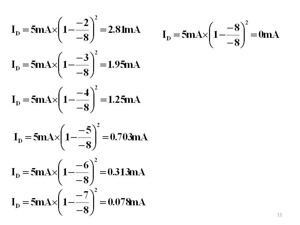
Example The following parameters are obtained from a certain JFET datasheet: VP = -8 v and IDSS = 5 mA. Determine the values of ID for each value of VGS ranging from 0 v to -8 v in 1 v steps. Plot the transfer characteristic curve from these data. Solution:

12
ID VGS

13
FET Biasing The following relations can be applied to the dc analysis of most of the FET amplifiers:

14
JFET Biasing: Fixed Bias Circuit

15
JFET Biasing: Fixed Bias Circuit
Circuit for dc analysis

16
Fixed Bias Circuit GS Loop: Apply KVL Apply the Shockley’s Equation:
Plot Shockley’s equation:

17
Fixed Bias Circuit Q-Point:

18
Fixed Bias Circuit DS Loop Also note that In addition

19
Example: Determine the following for the given Fig.
VGSQ (b) IDQ (c) VDS (d) VD (e) VG (f) VS. Solution: (a) VGSQ = -VGG = -2 V (b) (c) (d) VD = VDS = 4.75 V (e) VG = VGS = -2 V (f) VS = 0 V
 IDQ (c) VDS (d) VD (e) VG (f) VS. Solution: (a) VGSQ = -VGG = -2 V. (b) (c) (d) VD = VDS = 4.75 V. (e) VG = VGS = -2 V. (f) VS = 0 V.")
20
JFET Biasing: Self Bias Configuration

21
Self Bias Circuit: DC Analysis
Self-bias Circuit for dc analysis

22
JFET Self Bias Circuit IG = 0 IS = ID From GS Loop: -VGS = VRS or VGS = -ISRS Substituting IS = ID VGS = -IDRS.

23
JFET Self Bias Circuit Shockley Equation:

24
JFET Self Bias Circuit: Q-Point
Transfer Curve (Shockley equation) Self-Bias Line: Since VGS = -IDRS . If ID = 0 then VGS = 0 and ID = IDDS/2 (say), then VGS = -IDDS RS /2 Superimposing this straight line on the transfer curve, we get Q-point as shown in the Fig. Self Bias line
 Self-Bias Line: Since VGS = -IDRS . If ID = 0 then VGS = 0 and ID = IDDS/2 (say), then VGS = -IDDS RS /2 Superimposing this straight line on the transfer curve, we get Q-point as shown in the Fig. Self Bias line.")
25
JFET Self Bias Circuit DS Loop: Using KVL Substituting IS = ID, or In addition

26
JFET Self Bias Circuit: Example 1
Determine the following: VGSQ , IDQ, VDS, VS, VG, and VD. Solution: Step 1: Draw the self bias line: VGS = - IDRS , When ID = 0, VGS = 0. Choosing ID = 4 mA, VGS = -4mA×1 k = -4 v The line is drawn below:

27
JFET Self Bias Circuit: Example 1
Step 2: Plot the Shockley equation: (IDSS = 8mA, VP = -6v) VGS -1 -3 -4 -5 -6 ID (mA) 8 5.55 2 0.88 0.22 ID (mA) VGS (volts)
 VGS ID (mA) ID (mA) VGS (volts)")
28
JFET Self Bias Circuit: Example 1
Step 3: Show the Shockley curve and the self bias line on the same graph paper Shockley Curve Q-Point ID (mA) Self bias line VGS (volts) From the graph, VGSQ = -2.6 v, IDQ = 2.6 mA
 Self bias line. VGS (volts) From the graph, VGSQ = -2.6 v, IDQ = 2.6 mA.")
29
JFET Self Bias Circuit: Example 1
Step 4: Find the remaining quantities: VDS = VDD – ID(RS + RD ) = 20 – 2.6mA( 1 k k) = 8.82 v VS = IDRS = (2.6mA)(1k) = 2.6 v VG = 0 v VD = VDS + VS = = v (or VD = VDD – IDRD = v)
 = 20 – 2.6mA( 1 k k) = 8.82 v VS = IDRS = (2.6mA)(1k) = 2.6 v VG = 0 v VD = VDS + VS = = v (or VD = VDD – IDRD = v)")
30
JFET Biasing: Voltage Divider Circuit

31
JFET Biasing: Voltage Divider Circuit dc analysis
Applying KVL, VG or But VRS = ISRS = IDRS Therefore

32
Voltage Divider Circuit: Q-Point
Bias Line: (i) When ID = 0 VGS = VG – IDRS = VG – (0)(RS) VGS = VG (ii) When VGS = 0 Plot this line along with the Shockley Curve, as shown in the Figure.
 When ID = 0 VGS = VG – IDRS = VG – (0)(RS) VGS = VG (ii) When VGS = 0 Plot this line along with the Shockley Curve, as shown in the Figure.")
33
JFET Biasing: Voltage Divider Circuit dc analysis
From DS Loop: VG

34
Voltage Divider Circuit: Example
Determine the following: IDQ and VGSQ. VD VS VDS VDG.

35
Voltage Divider Circuit: Example 1
Solution: IDSS = 8 mA, Vp = -4 v. Shockley Equation: Bias Line: VGS -4 -2 -1 ID mA 2 4.5 8 When ID = 0, VGS = 1.82 v For VGS = 0, ID = 1.82/1.5k = 1.21 mA

36
From the Figure, IDQ = 2.4 mA, VGSQ = -1.8 v VD = VDD - IDRD = 16 – (2.4mA)(2.4k) = v (c) VS = IDRS = 16 – (2.4mA)(2.4k) = v (d) VDS = V DD – ID(RD + RS ) = 16 – (2.4mA)(2.4k + 1.5k) = 6.64 v (e) VDG = VD - VG = – 1.82 = 8.42 v
 VS = IDRS. = 16 – (2.4mA)(2.4k) = v. (d) VDS = V DD – ID(RD + RS ) = 16 – (2.4mA)(2.4k + 1.5k) = 6.64 v. (e) VDG = VD - VG = – 1.82 = 8.42 v.")
37
Voltage Divider Circuit: Example 2
For the given network, Detrmine VG. (b) IDQ and VGSQ. VD and VS. VDSQ . Solution: (a) (b) IDSS = 10mA, Vp = -3.5 v
 IDQ and VGSQ. VD and VS. VDSQ . Solution: (a) (b) IDSS = 10mA, Vp = -3.5 v.")
38
VGS (volts) -3.5 -2 -1 ID (mA) 1.8 5.1 10 Bias Line: VGS = VG – IDRS = 2.16 – ID(1.1k) When ID = 0, VGS = 2.6 v When VGS = 0, I = 2.16/1.1k = 2mA From the graph, we see that IDQ = 3.3 mA, VGSQ = -1.5 v (c) VD = VDD – IDQRD = (3.3mA)(2.2k) = v VS = IDRS = 3.63 v (d) VDSQ = VDD – IDQ(RD +RS ) = 9.11 v
 VD = VDD – IDQRD. = 20 - (3.3mA)(2.2k) = v. VS = IDRS = 3.63 v. (d) VDSQ = VDD – IDQ(RD +RS ) = 9.11 v.")
39
Metal-Oxide -Semiconductor Field Effect Transistor (MOSFET)
Depletion –Type MOSFET Enhancement-Type MOSFET

40
N- Channel Depletion-Type MOSFET
The foundation of this type of FET is the substrate (p-type material). The source and drain terminals are connected through metallic contacts to n doped regions linked by an n channel. The gate is also connected to a metal contact surface but remains insulated from the n-channel by a SiO2 layer. Construction of D-MOSFET (n-Channel)
. The source and drain terminals are connected through metallic contacts to n doped regions linked by an n channel. The gate is also connected to a metal contact surface but remains insulated from the n-channel by a SiO2 layer. Construction of D-MOSFET. (n-Channel)")
41
Basic Operation and Charactersitics of N – Channel D-MOSFET
When VGS = 0 and VDS is applied, the drain current ID = IDSS flows through the circuit due to the free electrons of the n-channel. VGS = 0 I D= I S= IDSS

42
Basic Operation and Characterstics of N-Channel D-MOSFET
When VGS < 0, recombination between electrons and holes occurs. The more negative the bias, the higher the rate of combination. The resulting level of ID is reduced and becomes zero at pinch-off voltage. Electrons repelled by negative Potential at gate.

43
Basic Operation and Charactersitics of D-MOSFET
When VGS > 0, the gate will draw additional electrons from the p-substrate due to the reverse leakage current and the drain current increases at a rapid rate.

44
Example: Sketch the transfer characteristics for an n-channel depletion type MOSFET with IDSS = 10 mA and Vp = -4 v. Solution: VGS -4 -2 -1 +1 ID (mA) 2.5 5.6 10 15.6 The curve is plotted on the next slide.
 The curve is plotted on the next slide.")
45
Drain Current (A) Gate Source Voltage
 Gate Source Voltage")
46
P-Channel depletion type MOSFET

47
Symbols P-Channel N-Channel

48
Example1: For the n-channel depletion type MOSFET of the Fig
Example1: For the n-channel depletion type MOSFET of the Fig., determine (a) IDQ and VGSQ. (b) VDS. Solution: Shockley Equation: 18 v VGS -3 -2 -1 1 ID (mA) 0.7 2.7 6 10.7
 IDQ and VGSQ. (b) VDS. Solution: Shockley Equation: 18 v. VGS ID (mA)")
49
Bias Line: When ID = 0, VGS = 1.5, When VGS = 0, ID = VG/RS = 1.5/750 = 2 mA From the graph, IDQ = 3.1 mA, VGSQ = -0.8 v VDS = VDD – ID(RD + RS) = 10.1 v
 = 10.1 v.")
50
Example2: Determine the following for the given network
Example2: Determine the following for the given network. (a) IDQ and VGSQ (b) VD. Solution: (a) Shockley Equation: VGS -8 -6 -5 -4 -2 1 2 ID(mA) 0.5 1.125 2.00 4.5 8.00 10.125 12.5
 IDQ and VGSQ (b) VD. Solution: (a) Shockley Equation: VGS ID(mA)")
51
From the graph paper VGSQ = 4.3 V, ID = 1.7mA (b) VD = VDD – ID RD = 20 – (1.7mA)(6.2k) = 9.46 V Bias Line: VGS = -IDRS. When VGS = 0, ID = 0. When ID = 2.5 mA (say) VGS = -2.510-3 2.4 1000 = -6V Shockley Equation ID (mA) Q-Point Bias Line VGS (volts)
 VGS = -2.510-3 2.4 1000 = -6V Shockley. Equation. ID (mA) Q-Point. Bias Line. VGS (volts)")
52
Example 3: For the following network, determine (a) IDQ and VGSQ (b) VDS and VS. Solution: Shockley Equation: VGS -8 -6 -5 -4 -2 1 2 ID(mA) 0.5 1.125 2.00 4.5 8.00 10.125 12.5
")
53
(b) VDS = VDD – IDQ(RD + RS) = 7.69 V VS = -VGSQ = -0.5V ID (mA)
Bias Line: VGS = -VSS – IDRS. When ID = 0 VGS = -(-4) = 4 V When VGS = 0 ID = -VSS/RS = 4/0.39k = mA From the graph VGSQ 0.5 V, IDQ 9mA (b) VDS = VDD – IDQ(RD + RS) = 7.69 V VS = -VGSQ = -0.5V Q-Point ID (mA) Shockley Equation Bias Line VGS (volts)
 = 4 V. When VGS = 0. ID = -VSS/RS = 4/0.39k = mA. From the graph. VGSQ 0.5 V, IDQ 9mA. (b) VDS = VDD – IDQ(RD + RS) = 7.69 V. VS = -VGSQ = -0.5V. Q-Point. ID (mA) Shockley Equation. Bias Line. VGS (volts)")
54
N-Channel Enhancement Type MOSFET
The construction of an enhancement type MOSFET is quite similar to that of the depletion type MOSFET except for the absence of a channel between the drain and source terminals. When VGS = 0, ID = 0 because the n-channel is absent.

55
Basic Operation and Characteristics of an n-Channel E-MOSFET
When VGS > 0 & VDS > 0, A depletion region is created near the SiO2 layer void of holes. As VGS increases, the concentration of electrons near the SiO2 increases and there is some flow between drain and source. The level of VGS that results in the significant increase in ID is called the Threshold Voltage (VT).
.")
56
Basic Operation and Characteristics of an n-Channel E-MOSFET
If VGS > VT is constant and VDS is increased, ID will Increase and will reach saturation.

57
Drain Characteristics of an n-channel enhancement-type MOSFET

58
Transfer characteristics for n-channel enhancement type MOSFET from the drain characteristics.
where

59
p-Channel enhancement-type MOSFET

60
Symbols

61
Feedback Biasing of n-Channel e-MOSFET
Equations: From the above equations, we get

62
Feedback Biasing of n-Channel e-MOSFET

63
Example: Determine IDQ and VDSQ for the enhancement-type MOSFET of the following. Solution: For the transfer curve VGS 3 6 8 10 ID 2.16mA 11.76mA

64
For the network bias line: For ID = 0, VGS = VDD = 12 v, and for VGS = 0 ID = VDD /ID = 12 v / 2k = 6 mA From the graph VGSQ = 6.4 v IDQ = 2.75 mA

65
Voltage Divider Bias Applying KVL around the indicated loop: or
For the output section:

66
Example: Determine IDQ and VDSQ for the given enhancement type MOSFET
Example: Determine IDQ and VDSQ for the given enhancement type MOSFET. Solution: Network: When VGS = 0, When ID = 0, VGS = 18 v

67
Device: From the graph VGSQ = 12.5 v IDQ = 6.7 mA VGS 5 10 15 20
ID (mA) 0.48 12 27 From the graph VGSQ = 12.5 v IDQ = 6.7 mA
 From the graph. VGSQ = 12.5 v. IDQ = 6.7 mA.")
68
Combination Networks Example1: Determine the levels of VD and VC for the given network: Solution:

69
Plot the following equation
From the plot, VGSQ = -3.7 v Now VC = VB – VGSQ = 3.62 – (-3.7) = 7.32 v
 = 7.32 v.")
70
Example 2: Determine VD for the given network.
Solution: From the JFET: VGS = -IDRS = -ID(2.4k) From this equation, the self Bias line is plotted as shown Below.
 From this equation, the self. Bias line is plotted as shown. Below.")
71
The resulting Q_point is at: VGSQ = -2
The resulting Q_point is at: VGSQ = -2.6 V, IDQ = 1mA For the BJT: IE IC = ID = 1mA IB = IC/ = 1mA/80 = 12.5A VB = VCC – IBRB = 16 – 12.5A470k = V VE = VD = VB – VBE = – 0.7 = V

72
Example 3: For the network of Fig
Example 3: For the network of Fig. (a), determine: VG , VGSQ, IDQ, IE, IB, VD and VC. Solution: VG = 3.3 V VGSQ = V IDQ = 3.75 mA IE = 3.75 mA IB = 23.44A VD = V VC = V Fig. (a)
, determine: VG , VGSQ, IDQ, IE, IB, VD and VC. Solution: VG = 3.3 V VGSQ = V IDQ = 3.75 mA IE = 3.75 mA IB = 23.44A VD = V VC = V Fig. (a)")
Similar presentations


>")

>")
>")
 EBB424E Dr. Sabar D. Hutagalung School of Materials & Mineral Resources Engineering, Universiti Sains Malaysia.>")
>")
>")

 Importance for LSI/VLSI –Low fabrication cost –Small size –Low power consumption Applications –Microprocessors –Memories.>")


>")

 by:- Uttampreet Singh Lecturer-Electrical Engg. Govt. Polytechnic College, G.T.B.garh, Moga.>")
 –3 layers of doped semiconductor –2 p-n junctions –Layers.>")