Download presentation
Presentation is loading. Please wait.

1
Prof. Sin-Min Lee Department of Computer Science
Lecture 14 CS 147 Cache Memory Prof. Sin-Min Lee Department of Computer Science

2
Memory: Capacity Word size: # of bits in natural unit of organization
Usually related to length of an instruction or the number of bits used to represent an integer number Capacity expressed as number of words or number of bytes Usually a power of 2, e.g. 1 KB 1024 bytes why?

3
Other Memory System Characteristics
Unit of Transfer: Number of bits read from, or written into memory at a time Internal : usually governed by data bus width External : usually a block of words e.g 512 or more Addressable unit: smallest location which can be uniquely addressed Internal : word or byte External : device dependent e.g. a disk “cluster”

4
Sequential Access Method
Start at the beginning – read through in order Access time depends on location of data and previous location e.g. tape start first location . . . read to here location of interest

5
Direct Access . . . Individual blocks have unique address
Access is by jumping to vicinity plus sequential search (or waiting! e.g. waiting for disk to rotate) Access time depends on target location and previous location e.g. disk . . . jump to here block i read to here
 Access time depends on target location and previous location. e.g. disk jump to here. block i. read to here.")
6
PRIMARY MEMORY The memory is that part of the computer where programs and data are stored. Some computer scientists (especially British ones) use the term store or storage rather than memory, although more and more, the term "storage" is used to refer to disk storage.
 use the term store or storage rather than memory, although more and more, the term storage is used to refer to disk storage.")
7
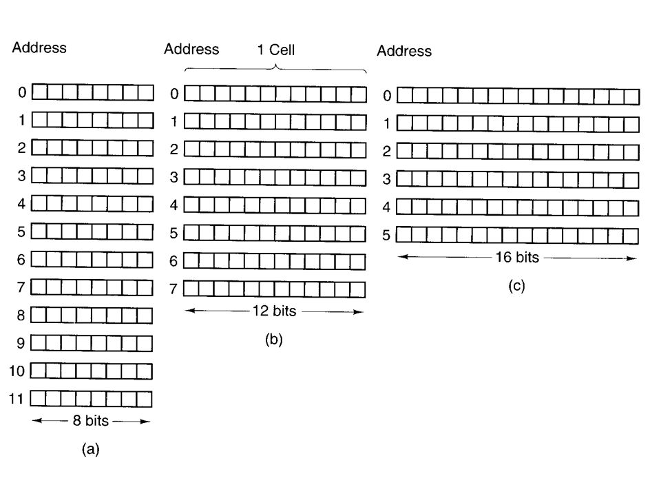
MEMORY ADDRESSES Memories consist of a number of cells (or locations) each of which can store a piece of information. Each cell has a number, called its address, by which programs can refer to it. If a memory has n cells, they will have addresses 0 to n - 1. All cells in a memory contain the same number of bits. If a cell consists of k bits, it can hold any one of 2k different bit combinations.

9
MEMORY ADDRESSES Computers that use the binary number system (including octal and hexadecimal notation for binary numbers) express memory addresses as binary numbers. If an address has m bits, the maximum number of cells addressable is 2m.
 express memory addresses as binary numbers. If an address has m bits, the maximum number of cells addressable is 2m.")
10
For example, an address used to reference the memory to the left needs at least 4 bits in order to express all the numbers from 0 to 11.

11
A 3-bit address is sufficient here
A 3-bit address is sufficient here. The number of bits in the address determines the maximum number of directly addressable cells in the memory and is independent of the number of bits per cell.

12
A memory with 212 cells of 8 bits each and a memory with 212 cells of 64 bits each each need 12-bit addresses. The number of bits per cell for some computers that have been sold commercially is listed to the right.

13
Random Access Method Individual addresses identify specific locations
Access time independent of location or previous access e.g. RAM main memory types . . . read here

14
Problem: CPU Fast, Memory Slow
After a memory request, the CPU will not get the word for several cycles Two simple solutions: Continue execution, but stall CPU if an instruction references the word before it has arrived (hardware) Require compiler to fetch words before they are needed (software) May need to insert NOP instructions Very difficult to write compilers to do this effectively
 Require compiler to fetch words before they are needed (software) May need to insert NOP instructions. Very difficult to write compilers to do this effectively.")
15
The Root of the Problem: Economics
Fast memory is possible, but to run at full speed, it needs to be located on the same chip as the CPU Very expensive Limits the size of the memory Do we choose: A small amount of fast memory? A large amount of slow memory? Problem increased by designers concentrating on making CPU’s faster and memories bigger

16
Memory Hierarchy Design (1)
Since 1987, microprocessors performance improved 55% per year and 35% until 1987 This picture shows the CPU performance against memory access time improvements over the years Clearly there is a processor-memory performance gap that computer architects must take care of

17
Memory Hierarchy Design (1)
Since 1987, microprocessors performance improved 55% per year and 35% until 1987 This picture shows the CPU performance against memory access time improvements over the years Clearly there is a processor-memory performance gap that computer architects must take care of

18
Memory Hierarchy Design (2)
It is a tradeoff between size, speed and cost and exploits the principle of locality. Register Fastest memory element; but small storage; very expensive Cache Fast and small compared to main memory; acts as a buffer between the CPU and main memory: it contains the most recent used memory locations (address and contents are recorded here) Main memory is the RAM of the system Disk storage - HDD
 Main memory is the RAM of the system. Disk storage - HDD.")
19
Memory Hierarchy Design (3)
Comparison between different types of memory Register Cache Memory HDD size: speed: $/Mbyte: B 2 ns 32KB - 4MB 4 ns $100/MB 128 MB 60 ns $1.50/MB 20 GB 8 ms $0.05/MB larger, slower, cheaper

20
The Best of Both Worlds: Cache Memory
Combine a small amount of fast memory (the cache) with a large amount of slow memory When a word is referenced, put it and its neighbours into the cache Programs do not access memory randomly Temporal Locality: recently accessed items are likely to be used again Spatial Locality: the next access is likely to be near the last one Early microprocessors had no cache; INMOS transputer was the 1st processor with on-chip cache; Acorn’s ARM (Acorn RISC Machine) was 1st processor to have dual level cache. Pentium II has 32KB L1 cache (16K for instructions; 16K for data); 512KB L2 cache (not on processor chip, but on separate chip within SEC cartridge, connected via dedicated bus).
 with a large amount of slow memory. When a word is referenced, put it and its neighbours into the cache. Programs do not access memory randomly. Temporal Locality: recently accessed items are likely to be used again. Spatial Locality: the next access is likely to be near the last one. Early microprocessors had no cache; INMOS transputer was the 1st processor with on-chip cache; Acorn’s ARM (Acorn RISC Machine) was 1st processor to have dual level cache. Pentium II has 32KB L1 cache (16K for instructions; 16K for data); 512KB L2 cache (not on processor chip, but on separate chip within SEC cartridge, connected via dedicated bus).")
21
The Cache Hit Ratio How often is a word found in the cache?
Suppose a word is accessed k times in a short interval 1 reference to main memory (k-1) references to the cache The cache hit ratio h is then
 references to the cache. The cache hit ratio h is then.")
22
Reasons why we use cache
Cache memory is made of STATIC RAM – a transistor based RAM that has very low access times (fast) STATIC RAM is however, very bulky and very expensive Main Memory is made of DYNAMIC RAM – a capacitor based RAM that has very high access times because it has to be constantly refreshed (slow) DYNAMIC RAM is much smaller and cheaper
 STATIC RAM is however, very bulky and very expensive. Main Memory is made of DYNAMIC RAM – a capacitor based RAM that has very high access times because it has to be constantly refreshed (slow) DYNAMIC RAM is much smaller and cheaper.")
23
Performance (Speed) Access time Memory cycle time Transfer rate
Time between presenting the address and getting the valid data (memory or other storage) Memory cycle time Some time may be required for the memory to “recover” before next access cycle time = access + recovery Transfer rate rate at which data can be moved for random access memory = 1 / cycle time (cycle time)-1
 Memory cycle time. Some time may be required for the memory to recover before next access. cycle time = access + recovery. Transfer rate. rate at which data can be moved. for random access memory = 1 / cycle time. (cycle time)-1.")
24
Memory Hierarchy size ? speed ? cost ? registers internal
in CPU internal may include one or more levels of cache external memory backing store smallest, fastest, most expensive, most frequently accessed medium, quick, price varies largest, slowest, cheapest, least frequently accessed

25
Memory: Location Registers: inside cpu Internal or main memory
Fastest – on CPU chip Cache : very fast, semiconductor, close to CPU Internal or main memory Typically semiconductor media (transistors) Fast, random access, on system bus External or secondary memory peripheral storage devices (e.g. disk, tape) Slower, often magnetic media , maybe slower bus
 Fast, random access, on system bus. External or secondary memory. peripheral storage devices (e.g. disk, tape) Slower, often magnetic media , maybe slower bus.")
26
Memory Hierarchy - Diagram
decreasing cost per bit, speed, access frequency increasing capacity, access time

27
Performance & Hierarchy List
Registers Level 1 Cache Level 2 Cache Main memory Disk cache Disk Optical Tape Faster, +$/byte soon ( 2 slides ! ) Slower, -$/byte
 Slower, -$/byte.")
28
Locality of Reference (circa 1968)
During program execution memory references tend to cluster, e.g. loops Many instructions in localized areas of pgm are executed repeatedly during some time period, and remainder of pgm is accessed infrequently. (Tanenbaum) Temporal LOR: a recently executed instruction is likely to be executed again soon Spatial LOR: instructions with addresses close to a recently executed instruction are likely to be executed soon. Same principles apply to data references.
 Temporal LOR: a recently executed instruction is likely to be executed again soon. Spatial LOR: instructions with addresses close to a recently executed instruction are likely to be executed soon. Same principles apply to data references.")
29
Cache small amount of fast memory
smaller than main memory small amount of fast memory sits between normal main memory and CPU may be located on CPU chip or module cache views main memory as organized in “blocks” block transfer word transfer cache

30
The Cache Hit Ratio How often is a word found in the cache?
Suppose a word is accessed k times in a short interval 1 reference to main memory (k-1) references to the cache The cache hit ratio h is then
 references to the cache. The cache hit ratio h is then.")
31
Mean Access Time Cache access time = c Main memory access time = m
Mean access time = c +(1-h)m If all address references are satisfied by the cache, the access time approaches c If no reference is in the cache, the access time approaches c+m
m. If all address references are satisfied by the cache, the access time approaches c. If no reference is in the cache, the access time approaches c+m.")
32
Cache Design Issues How big should the cache be?
Bigger means more hits, but more expensive How big should a cache-line be? How does the cache keep track of what it contains? If we change an item in the cache, how do we write it back to main memory? Separate caches for data and instructions? Instructions never have to be written back to main memory How many caches should there be? Primary (on chip), secondary (off chip), tertiary…
, secondary (off chip), tertiary…")
33
Why does Caching Improve Speed?
Example: Main memory has 100,000 words, access time is 0.1 s. Cache has 1000 words and access time is 0.01 s. If word is in cache (hit), it can be accessed directly by processor. in memory (miss), it must be first transferred to cache before access. Suppose that 95% of access requests are hits. Average time to access a word (0.95)(0.01 s)+0.05(0.1 s s) = s Key proviso Close to cache speed
, it can be accessed directly by processor. in memory (miss), it must be first transferred to cache before access. Suppose that 95% of access requests are hits. Average time to access a word (0.95)(0.01 s)+0.05(0.1 s s) = s. Key proviso. Close to cache speed.")
34
Cache Read Operation CPU requests contents of memory location
check cache for contents of location cache hit ! present get data from cache (fast) cache miss ! not present read required block from main to cache then deliver data from cache to CPU
 cache miss ! not present read required block from main to cache. then deliver data from cache to CPU.")
35
Cache Design Size Mapping Function Replacement Algorithm Write Policy
Block Size Number of Caches

36
Size Cost Speed More cache is expensive
More cache is faster (up to a point) Checking cache for data takes time
 Checking cache for data takes time.")
37
identify block address
Mapping Function how does cache contents map to main memory contents? cache tag data block main memory address contents 000 xxx line blocki . . . blockj use tag (and maybe line address) to identify block address
 to. identify block address.")
38
Cache Basics cache line width bigger than memory location
cache line vs. main memory location same concept – avoid confusion (?) line has address and contents contents of cache line divided into tag and data fields fixed width fields used differently ! data field holds contents of a block of main memory tag field helps identify the start address of the block of memory that is in the data field
 line has address and contents. contents of cache line divided into tag and data fields. fixed width. fields used differently ! data field holds contents of a block of main memory. tag field helps identify the start address of the block of memory that is in the data field.")
39
Cache (2) Every address reference goes first to the cache;
if the desired address is not here, then we have a cache miss; The contents are fetched from main memory into the indicated CPU register and the content is also saved into the cache memory If the desired data is in the cache, then we have a cache hit The desired data is brought from the cache, at very high speed (low access time) Most software exhibits temporal locality of access, meaning that it is likely that same address will be used again soon, and if so, the address will be found in the cache Transfers between main memory and cache occur at granularity of cache lines or cache blocks, around 32 or 64 bytes (rather than bytes or processor words). Burst transfers of this kind receive hardware support and exploit spatial locality of access to the cache (future access are often to address near to the previous one)
 Most software exhibits temporal locality of access, meaning that it is likely that same address will be used again soon, and if so, the address will be found in the cache. Transfers between main memory and cache occur at granularity of cache lines or cache blocks, around 32 or 64 bytes (rather than bytes or processor words). Burst transfers of this kind receive hardware support and exploit spatial locality of access to the cache (future access are often to address near to the previous one)")
40
Where can a block be placed in Cache? (1)
Real caches contain hundreds of block frames and real memories contain millions of blocks. Those numbers are chosen for simplicity. Assume that there is nothing in the cache and the block address in question (address that is accessed by processor falls within the block address number 12 in the main memory), then we can have three types of caches (from a block placement point of view): Fully associative – where block 12 from the lower level memory can go into any of 8 block frames of the cache Direct mapped – where block 12 from the lower level memory can go only into block frame 4 (12 mod 8) Set associative – where block 12 from the lower level memory can go anywhere into set 0 (12 mod 4, if our memory has four sets). With two blocks per set, that means that the block 12 can go anywhere into block frame 0 or block frame 1 of the cache. Our cache has eight block frames and the main memory has 32 blocks
, then we can have three types of caches (from a block placement point of view): Fully associative – where block 12 from the lower level memory can go into any of 8 block frames of the cache. Direct mapped – where block 12 from the lower level memory can go only into block frame 4 (12 mod 8) Set associative – where block 12 from the lower level memory can go anywhere into set 0 (12 mod 4, if our memory has four sets). With two blocks per set, that means that the block 12 can go anywhere into block frame 0 or block frame 1 of the cache. Our cache has eight block frames and the main memory has 32 blocks.")
41
Where can a block be placed in Cache? (2)
Direct mapped Cache Each block has only one place where it can appear in the cache (Block Address) MOD (Number of blocks in cache) Fully associative Cache A block can be placed anywhere in the cache Set associative Cache A block can be placed in a restricted set of places into the cache A set is a group of blocks into the cache (Block Address) MOD (Number of sets in the cache) If there are n blocks in the cache, the placement is said to be n-way set associative
 MOD (Number of blocks in cache) Fully associative Cache. A block can be placed anywhere in the cache. Set associative Cache. A block can be placed in a restricted set of places into the cache. A set is a group of blocks into the cache. (Block Address) MOD (Number of sets in the cache) If there are n blocks in the cache, the placement is said to be n-way set associative.")
42
Mapping Function Example
holds up to 64 Kbytes of main memory contents cache of 64 KByte 16 K (214) lines – each line is 5 bytes wide = 40 bits 16 MBytes main memory 24 bit address 224 = 16 M will consider DIRECT and ASSOCIATIVE mappings tag field: 1 byte 4 byte blocks of main memory data field: 4 bytes
 lines – each line is 5 bytes wide = 40 bits. 16 MBytes main memory. 24 bit address. 224 = 16 M. will consider DIRECT and ASSOCIATIVE mappings. tag field: 1 byte. 4 byte blocks. of main memory. data field: 4 bytes.")
43
Direct Mapping address s w line field identifies line s containing
each block of main memory maps to only one cache line i.e. if a block is in cache, it must be in one specific place – based on address! split address into two parts least significant w bits identify unique word in block most significant s bits specify one memory block split s bits into: cache line address field r bits tag field of s-r most significant bits address s w line field identifies line containing block ! s tag line s – r r

44
Direct Mapping: Address Structure for Example
24 bit address word w tag s-r line address r 8 14 2 2 bit word identifier (4 byte block) s = 22 bit block identifier two blocks may have the same r value, but then always have different tag value !
 s = 22 bit block identifier. two blocks may have the same r value, but then always have different tag value !")
45
Direct Mapping Cache Line Table
each block = 4 bytes cache line main memory blocks held , m, 2m, 3m, … 2s-m , m+1, 2m+1, … 2s-m+1 m-1 m-1, 2m-1,3m-1, … 2s-1 . . . . . . s=22 m=214 But…a line can contain only one of these at a time!

46
Direct Mapping Cache Organization

47
Direct Mapping pros & cons
Simple Inexpensive Fixed location for given block If a program accesses 2 blocks that map to the same line repeatedly, cache misses are very high

48
Associative Memory read: specify tag field value and word select
checks all lines – finds matching tag return contents of data selected word access time independent of location or previous access write to data tag value + word select what if no words with matching tag?

49
s = tag does not use line address !
Associative Mapping main memory block can load into any line of cache memory address is interpreted as tag and word select in block tag uniquely identifies block of memory ! every line’s tag is examined for a match cache searching gets expensive s = tag does not use line address !

50
Fully Associative Cache Organization
no line field !

51
Associative Mapping Example
tag = most signif. 22 bits of address Typo- leading F missing!

52
Associative Mapping Address Structure
Word 2 bit Tag 22 bit 22 bit tag stored with each 32 bit block of data Compare tag field with tag entry in cache to check for hit Least significant 2 bits of address identify which 8 bit word is required from 32 bit data block e.g. Address Tag Data Cache line FFFFFC 3FFFFF any, e.g. 3FFF

53
Set Associative Mapping
Cache is divided into a number of sets Each set contains k lines k – way associative A given block maps to any line in a given set e.g. Block B can be in any line of set i e.g. 2 lines per set 2 – way associative mapping A given block can be in one of 2 lines in only one set

54
K-Way Set Associative Cache Organization
Direct + Associative Mapping set select (direct) tag (associative)
 tag. (associative)")
55
Set Associative Mapping Address Structure
Word 2 bit Tag 9 bit Set 13 bit Use set field to determine which set of cache lines to look in (direct) Within this set, compare tag fields to see if we have a hit (associative) e.g Address Tag Data Set number FFFFFC 1FF FFF 00FFFF FFF Same Set, different Tag, different Word
 Within this set, compare tag fields to see if we have a hit (associative) e.g. Address Tag Data Set number. FFFFFC 1FF FFF. 00FFFF FFF. Same Set, different Tag, different Word.")
56
e.g Breaking into Tag, Set, Word
Given Tag=9 bits, Set=13 bits, Word=2 bits Given address FFFFFD16 What are values of Tag, Set, Word? First 9 bits are Tag, next 13 are Set, next 2 are Word Rewrite address in base 2: Group each field in groups of 4 bits starting at right Add zero bits as necessary to leftmost group of bits 1FF 1FFF (Tag, Set, Word)
")
57
Replacement Algorithms Direct Mapping
what if bringing in a new block, but no line available in cache? must replace (overwrite) a line – which one? direct no choice each block only maps to one line replace that line
 a line – which one direct no choice. each block only maps to one line. replace that line.")
58
Replacement Algorithms Associative & Set Associative
hardware implemented algorithm (speed) Least Recently Used (LRU) e.g. in 2-way set associative which of the 2 blocks is LRU? First In first Out (FIFO) replace block that has been in cache longest Least Frequently Used (LFU) replace block which has had fewest hits Random
 Least Recently Used (LRU) e.g. in 2-way set associative. which of the 2 blocks is LRU First In first Out (FIFO) replace block that has been in cache longest. Least Frequently Used (LFU) replace block which has had fewest hits. Random.")
59
Write Policy must not overwrite a cache block unless main memory is up to date Complication: Multiple CPUs may have individual caches!! Complication: I/O may address main memory too (read and write)!! N.B. 15% of memory references are writes
!! N.B. 15% of memory references are writes.")
60
Write Through Method all writes go to main memory as well as cache
Each of multiple CPUs can monitor main memory traffic to keep its own local cache up to date lots of traffic slows down writes

61
Write Back Method updates initially made in cache only
update (dirty) bit for cache slot is set when update occurs if block is to be replaced, write to main memory only if update bit is set Other caches get out of sync I/O must access main memory through cache
 bit for cache slot is set when update occurs. if block is to be replaced, write to main memory only if update bit is set. Other caches get out of sync. I/O must access main memory through cache.")
62
Multiple Caches on one processor
two levels – L1 close to processor (often on chip) L2 – between L1 and main memory check L1 first – if miss – then check L2 if L2 miss – get from memory processor L1 L2 local bus system bus to high speed bus
 L2 – between L1 and main memory. check L1 first – if miss – then check L2. if L2 miss – get from memory. processor. L1. L2. local. bus. system bus. to high speed bus.")
63
Unified vs. Split Caches
unified both instruction and data in same cache split separate caches for instructions and data separate local busses to cache increased concurrency pipelining allows instruction fetch to be concurrent with operand access

64
Pentium Family Cache Evolution
80386 – no on chip cache 80486 – 8k using 16 byte lines and four way set associative organization Pentium (all versions) – two on chip L1 (split) caches data & instructions
 – two on chip L1 (split) caches. data & instructions.")
65
Pentium 4 Cache Pentium 4 – split L1 caches 8k bytes
128 lines of 64 bytes each four way set associative = 32 sets unified L2 cache – feeding both L1 caches 256k bytes 2048 (2k) lines of 128 bytes each 8 way set associative = 256 sets how many bits ? w words s set
 lines of 128 bytes each. 8 way set associative = 256 sets. how many bits w words. s set.")
66
Pentium 4 Diagram (Simplified)
L1 instructions unified L2 L1 data

67
Power PC Cache Evolution
601 – single 32kb 8 way set associative 603 – 16kb (2 x 8kb) two way set associative 604 – 32kb 610 – 64kb G3 & G4 64kb L1 cache 8 way set associative 256k, 512k or 1M L2 cache two way set associative
 two way set associative. 604 – 32kb. 610 – 64kb. G3 & G4. 64kb L1 cache 8 way set associative. 256k, 512k or 1M L2 cache two way set associative.")
68
PowerPC G4 L1 instructions unified L2 L1 data

69
CACHE MEMORY Historically, CPUs have always been faster than memories.
As memories have improved, so have CPUs, preserving the imbalance. In fact, as it becomes possible to put more and more circuits on a chip, CPU designers are using these new facilities for pipelining and superscalar operation, making CPUs go even faster. Memory designers have usually used new technology to increase the capacity of their chips, not the speed, so the problem appears to be getting worse in time.

70
CACHE MEMORY What this imbalance means in practice is that after the CPU issues a memory request, it will not get the word it needs for many CPU cycles. The slower the memory, the more cycles the CPU will have to wait.

71
CACHE MEMORY Actually, the problem is not technology, but economics.
Engineers know how to build memories that are as fast as CPUs, but to run at full speed, they have to be located on the CPU chip (because going over the bus to memory is very slow).
.")
72
CACHE MEMORY Putting a large memory on the CPU chip makes it bigger, which makes it more expensive, and even if cost were not an issue, there are limits to how big a CPU chip can be made. Thus the choice comes down to having a small amount of fast memory or a large amount of slow memory. What we would prefer is a large amount of fast memory at a low price.

73
How it works Whenever the processor requires access to data or an instruction stored in RAM, it makes a request to a particular memory address The Cache Controller intercepts this request and checks cache memory to see if that address is stored in cache. If it is, the Cache Controller directs the CPU to access the faster Cache Ram instead. If it does not exist, then the cache controller instructs the CPU to write the contents of that address into the Cache so that the next time it is requested it will be in Cache for the CPU’s use.

74
Organization is the key
A good Cache system has to be able to do the following: Find information quickly (Search Times -- Low is good) Keep data long enough to be used KB isn’t a lot of memory (Hit Rates -- High is good) It’s pretty easy to do one or the other, but not so easy to do both.
 Keep data long enough to be used KB isn’t a lot of memory (Hit Rates -- High is good) It’s pretty easy to do one or the other, but not so easy to do both.")
75
What’s a line? Often Main Memory and Cache Memory cells that store data are called “Lines.” Each line holds a piece of data or instruction and has an address associated with it. Although it is up to the designers of the cache system to decide how long these lines are, today they are 32 bytes.

76
Direct Mapped Cache Direct Mapped Cache divides the Cache memory into as many lines as it can and then it assigns each line to a “block” of Main Memory lines

77
Do until A=5 A=A+1 Print A END LOOP Do until A=5

78
Do until A=5 A=A+1 Print A END LOOP A=A+1

79
Do until A=5 A=A+1 Print A END LOOP Print A

80
Do until A=5 A=A+1 Print A END LOOP END LOOP

81
Direct Mapped Cache Because there is such high competition for space, data is replaced in the Cache often and therefore, the data we require is seldom (if ever) present in Cache when we need it -- LOW HIT RATES = BAD The advantage of this type of organization is that there is only one place to look for any given address and that makes the cache system very fast -- LOW SEARCH TIMES = GOOD
 present in Cache when we need it -- LOW HIT RATES = BAD. The advantage of this type of organization is that there is only one place to look for any given address and that makes the cache system very fast -- LOW SEARCH TIMES = GOOD.")
82
Fully Associative Cache
In a Fully Associative Cache, the Cache is divided into as many lines as possible and the Main Memory is divided into as many lines as possible. There is no assigning of lines at all. Any line from Main Memory can be stored on any line of Cache.

83
Do until A=5 A=A+1 Print A END LOOP Do until A=5

84
Do until A=5 A=A+1 Print A END LOOP Do until A=5 A=A+1

85
Do until A=5 A=A+1 Print A END LOOP Do until A=5 A=A+1 Print A END LOOP

86
Fully Associative Cache
The previous scenario at first seems to work really well – after a single Main Memory access to each line, we can retrieve each line from Cache for subsequent accesses (HIGH HIT RATE = GOOD) The problem however, is that the Cache controller has no way of knowing exactly where the data is and therefore must search through the entire Cache until it finds what it is looking for, taking up a lot of precious time (HIGH SEARCH TIMES = BAD)
 The problem however, is that the Cache controller has no way of knowing exactly where the data is and therefore must search through the entire Cache until it finds what it is looking for, taking up a lot of precious time (HIGH SEARCH TIMES = BAD)")
87
A third problem… (which we’ll talk about later)
What happens if the cache fills up? We need to decide what gets discarded and depending on the Replacement Policy that is used, this can have an impact on the performance

88
N-WAY Set Associative An N-WAY Set associative cache tries to find a middle ground compromise between the previous two strategies – In fact, Direct Mapped and Fully Associative strategies are simply two extreme cases of N-WAY Set! The “N” in N-WAY actually represents a number (2,4,8,etc.) The following example deals with a 2-WAY Set Associative organization. The Cache is broken up into groups of two (2) lines and then Main Memory is divided into the same number of groups that exist in the Cache. Each group in Cache is assigned to a group Main Memory.
 The following example deals with a 2-WAY Set Associative organization. The Cache is broken up into groups of two (2) lines and then Main Memory is divided into the same number of groups that exist in the Cache. Each group in Cache is assigned to a group Main Memory.")
89
Do until A=5 A=A+1 Print A END LOOP Do until A=5 A=A+1

90
N-WAY Set Associative Due to the fact that there is less competition for space in the Cache, there is a higher chance of getting the data you want – AS N INCREASES, HIT RATES GET HIGHER = GOOD However, there is more than one line to search and therefore there is more time involved in finding data – AS N INCREASES, SEARCH TIMES GET HIGHER = BAD There is still the problem of what data to replace and what the impacts on performance will be

91
Let’s Split Any of these Cache organizations can be Split or Unified If a Cache is split, it means that half of the Cache is used to store instructions only, and the other half is used to store data created by programs Advantage – It’s more organized and easier to find what you’re looking for Disadvantage – Instructions are generally much smaller than the data produced by a program, so a lot of space can be wasted

92
A Final Word Cache organizations are not something you can tweak – they are determined by the manufacturer through research on current software packages and benchmarks vs. the amount of memory available on the chip Intel and AMD processors currently use a Split 8 - way L1 cache and a unified 8 - way L2 cache You may have heard by now of the Intel L3 cache on the Itanium processor. This is simply another layer of memory that works in conjunction with the L1 and L2 cache. It is not on the die of the processor, but still works faster than Main Memory and is larger than L1 or L2 so it is still quite effective

Similar presentations


 Tag.>")


 - Asim LUMS 1 Cache Basics Adapted from a presentation by Beth Richardson>")


 that a computer microprocessor can access more quickly than it can access.>")
