Download presentation
Presentation is loading. Please wait.

1
Checkpoint 3 To Do Hints General Debugging

2
To Do: Before Lab Plan layout of chips Wire sync separator, A/D, op amp and RC network Enter and simulate FSM to store one video frame in SRAM (either 196x210 or 14x10)
")
4
Video Signal

5
Begin frame: “Wait 17 horizontal periods after vertical sync. goes low.” –VBLANK.H = active high VERT_SYNC Begin row: “Wait 9.5 usec after composite sync. goes low” –9.5 usec = 4.7 usec + 4.8 usec Ex: 52.4 usec / 14 = sample every 3.75 usec Ex: 241 lines / 10 = sample every 24 lines

6
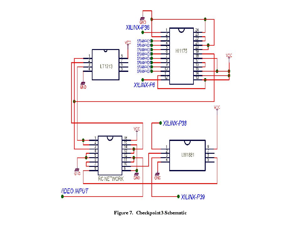
From wvlib\cs150\check3.sch

7
Two Cycle Write 52.4 usec / 196 = 0.27 usec 10 MHz CLK = 0.1 usec per cycle Only have 1/2 cycle for stable ADDR CLK WEWE_OUT OFD_1 OPADDQ LOC=P14

8
OE, UART_OE, AD_OE Now have three registers on D bus Add separate UART_OE. Change: Old lab9pinout.schChange lab9pinout.sch:

9
OE, UART_OE, AD_OE, cont. Add OFD to OE (if you haven’t already) Add AD_OE (already in check3.sch):
 Add AD_OE (already in check3.sch):")
10
Processing A/D data While reading A/D: send directly to SRAM During PWM: shift from 8 bit to 5 bit Also, adjust to min/max A/D values

11
To Do: In Lab Test camera on television Look at video signal on oscilloscope Test bit file u:wvlib\cs150\check3.bit

12
To Do: Check Your Circuit View comp. sync. and WE –should see 14 or 196 WE per comp.sync. View vert. sync., WE and ROW_INC –should see WE pulse block between syncs. –should see 10 or 210 ROW_INC per vert sync.

13
To Do: Checkoffs Valid comp. and vert. sync. from LM1881 Show A/D CLK and D[7:0] and SRAM WE on oscilloscope

14
Hints Save CLBs: remove LED_BLOCK, ROM Modularize each FSM: reset, enable, done: UART_RESET UART_ENABLE CLK SERIAL_CLEAN RESET ENABLE CLK SERIAL_CLEAN DONE DATA[7:0] UART_DONE UARTDATA[7:0] CLK NS0PS0 FDRE DQ ENABLECE RESETR
![Hints Save CLBs: remove LED_BLOCK, ROM Modularize each FSM: reset, enable, done: UART_RESET UART_ENABLE CLK SERIAL_CLEAN RESET ENABLE CLK SERIAL_CLEAN DONE DATA[7:0] UART_DONE UARTDATA[7:0] CLK NS0PS0 FDRE DQ ENABLECE RESETR](http://images.slideplayer.com/16/4985778/slides/slide_14.jpg "Hints Save CLBs: remove LED_BLOCK, ROM Modularize each FSM: reset, enable, done: UART_RESET UART_ENABLE CLK SERIAL_CLEAN RESET ENABLE CLK SERIAL_CLEAN DONE DATA[7:0] UART_DONE UARTDATA[7:0] CLK NS0PS0 FDRE DQ ENABLECE RESETR")
15
General Debugging Get simplest part working: Example: checkpoint 2 –Light up all LEDs on row 3 –Light up all LEDs with intensity 16 –receive one byte from PTEST.EXE (^A = 0x01) and light up all LEDs
 and light up all LEDs")
16
General Debugging Implementation log: –“No load on xxx” is OK –“No driver on xxx” not OK “I can’t find the part giving the error!”: –1. Make a copy of schematics –2. Rip out sections and re-implement until error goes away –3. Add sections back in: ISOLATE.

17
General Debugging Don’t assume equipment works: –“This pin is always zero”: Does the oscilloscope even work? Try touching +5V –“My RS232 Rout has no output”: Does it have an input? Is anything coming down the serial cable? (Test just the serial cable (after testing your scope probe on +5V (after testing that your power supply puts out +5V)))
)).")
18
General Debugging Make the simulation work first Use NUMLED1 to watch counters Make a new counter and watch on NUMLED1 Use the oscilloscope! –Send signals to ERROR, NUMLED1 pins –Use “single” trigger to catch event

19
General Debugging Make sure you read about Xilinx part before you use it. (Ex: CD8RE) Read the newsgroup –(If you don’t know how, you’re an engineer: Find out) SIMPLIFY and ISOLATE
 Read the newsgroup –(If you don’t know how, you’re an engineer: Find out) SIMPLIFY and ISOLATE.")
Similar presentations


 Digital multimeter (DMM) Power Supply Signal Generator Oscilloscope.>")


 Group #1 Lee Estep Philip Robertson Andy Schiestl Robert Tate.>")


![[M2] Traffic Control Group 2 Chun Han Chen Timothy Kwan Tom Bolds Shang Yi Lin Manager Randal Hong Wed. Oct. 27 Overall Project Objective : Dynamic Control.](/16/5037070/big_thumb.jpg "[M2] Traffic Control Group 2 Chun Han Chen Timothy Kwan Tom Bolds Shang Yi Lin Manager Randal Hong Wed. Oct. 27 Overall Project Objective : Dynamic Control.>")

![[M2] Traffic Control Group 2 Chun Han Chen Timothy Kwan Tom Bolds Shang Yi Lin Manager Randal Hong Mon. Nov. 11 Overall Project Objective : Dynamic Control.](/16/5065559/big_thumb.jpg "[M2] Traffic Control Group 2 Chun Han Chen Timothy Kwan Tom Bolds Shang Yi Lin Manager Randal Hong Mon. Nov. 11 Overall Project Objective : Dynamic Control.>")


