Download presentation
Presentation is loading. Please wait.

1
Mammography Physics Jerry Allison, Ph.D. Department of Radiology
Medical College of Georgia Georgia Regents University Augusta, GA

2
Educational Objectives
Our educational objectives are to understand: 1. Why pay special attention to mammography physics? 2. Radiation Risk/Benefit Issues 3. Physical principles of mammography 4. Physical principles of full field digital mammography (FFDM) 5. Technical Details of Digital Breast Tomosynthesis (DBT)
 5. Technical Details of Digital Breast Tomosynthesis (DBT)")
3
Why pay special attention to mammography physics?
Approximately 1 of 8 women will develop breast cancer over a lifetime. 10-30% of women who have breast cancer have negative mammograms. ~80% of masses biopsied are not malignant (fibroadenomas, small papillomas, proliferating dysplasia). Fibroadenoma – lumps of fibrous and glandular material (benign) Papilloma – benign tumor Proliferating dysplasia – increased cell growth (benign but may be a risk factor)
. Fibroadenoma – lumps of fibrous and glandular material (benign) Papilloma – benign tumor. Proliferating dysplasia – increased cell growth (benign but may be a risk factor)")
4
Radiation Risk/Benefit Issues
Radiation is a carcinogen (ionizing radiation, x-radiation, radiation: National Toxicology Program 2004) "No woman has been shown to have developed breast cancer as a result of mammography, not even from multiple studies performed over many years with doses higher than the current dose (250 mRad)... However the possibility of such risk has been raised because of excessive incidence of breast cancer in women exposed to much higher doses ( Rad: Japanese A-bomb survivors, TB patients having chest fluoro and postpartum mastitis patients treated w/radiation therapy).” ©1992 RSNA
 No woman has been shown to have developed breast cancer as a result of mammography, not even from multiple studies performed over many years with doses higher than the current dose (250 mRad)... However the possibility of such risk has been raised because of excessive incidence of breast cancer in women exposed to much higher doses ( Rad: Japanese A-bomb survivors, TB patients having chest fluoro and postpartum mastitis patients treated w/radiation therapy). ©1992 RSNA.")
5
Risk/Benefit ©NCRP 2006 (Report 149)
Excess cases – note that breast radiation induced breast cancer has a long latency ©NCRP 2006 (Report 149)
")
6
Breast Tissue Composition
Lineart attenuation: a function of Z cubed and 1/(E cubed) Atomic numbers – C 6, Ca 20, H 1, O 8 ©1992 RSNA
 Atomic numbers – C 6, Ca 20, H 1, O 8. ©1992 RSNA.")
7
The Challenge in Mammography
©1987 IOP Publishing

8
kV Dependence An increase in kV: Reduces subject contrast
Reduces exposure time Reduced motion artifact

9
Mammography performed from ~23 to ~32 kVp
©1993 RSNA

10
X-ray Spectra in Mammography
X-ray spectral distribution is determined by: kV target/filter combination Mo/Mo, Mo/Rh, Rh/Rh for GE Mo/Mo, Mo/Rh, W/Rh for Siemens Mo/Mo, Mo/Rh or W/Rh, W/Ag for Hologic W/Rh, W/Ag, W/Al for Hologic DBT Tomo W/Rh for Giotto W/Rh for Fuji Sapire HD W/Rh, W/Ag for Planmed W/Al for Philips Hologic DBT uses an Al filter for tomo

11
X-ray spectra are variable

12
Compression (Redistribution?)
Scatter Geometric blurring Superposition Increases the proportion of the X-ray beam that is used to image a breast Motion Beam hardening Dose Beam hardening – HVL for a mammography beam is ~1-2 cm of soft tissue Lower energy photons are preferentially removed from the beam first, increasing the average beam energy (and reducing image contrast) as the beam passes through more breast thickness ©1994 Williams & Wilkins
 as the beam passes through more breast thickness. ©1994 Williams & Wilkins.")
13
Scattered Radiation Control
Only 40-75% of the possible contrast is imaged in mammography unless scatter is controlled. Mammography grids transmit 60-70% of primary X-rays and absorb 75-85% of scattered X-rays.

14
Scattered Radiation Control
Linear Grids Grid ratio (height of lamina/distance between laminae): 4:1 or 5:1 w/ lines/cm. Conventional grids are 8:1 to 12:1 (up to 43 lines/cm). Breast dose is increased by grids (Bucky Factor: x2 to x3) w/40% improvement in contrast. Laminae are focused to the focal spot to prevent grid cut off. Lead strips reciprocate left to right during a mammographic exposure Linear grids remove scatter one dimensionally (photons that are scattered left to right, but not photons that are scattered A to P)
: 4:1 or 5:1 w/ lines/cm. Conventional grids are 8:1 to 12:1 (up to 43 lines/cm). Breast dose is increased by grids (Bucky Factor: x2 to x3) w/40% improvement in contrast. Laminae are focused to the focal spot to prevent grid cut off. Lead strips reciprocate left to right during a mammographic exposure. Linear grids remove scatter one dimensionally (photons that are scattered left to right, but not photons that are scattered A to P)")
15
Scattered Radiation Control
High Transmission Cellular (HTC) Grids Focused Increased 2D absorption of scattered radiation Increase contrast Must move the grid a very precise distance during exposure regardless of exposure duration Essentially same grid ratio and dose as conventional linear grids
 Grids. Focused. Increased 2D absorption of scattered radiation. Increase contrast. Must move the grid a very precise distance during exposure regardless of exposure duration. Essentially same grid ratio and dose as conventional linear grids.")
16
HTC Grid

17
HTC Grid

18
Magnification Increased effective resolution by the magnification factor. Magnification factor: x1.5 – x2.0 Effective resolution describes the enlargement of the X-ray pattern relative to the unsharpness of the image receptor.

19
Contact mammogram – breast placed on top of the image receptor
©1994 Williams & Wilkins

20
Magnification Spot compression paddles

21
Magnification Reduction of effective image noise (less quantum noise, more photons per object area) Air gap between breast and image receptor reduces scattered radiation without attenuating primary photons or increasing radiation dose (no grid!) Small focal spot: mm (low mA, long exposure times) Increased dose (x2-x3)
 Small focal spot: mm (low mA, long exposure times) Increased dose (x2-x3)")
22
Focal Spot and Screen-Film MTF
Ttraditional radiographic x-ray units have focal spots of ~1.2mm and ~0.6mm ©1994 Williams & Wilkins

23
Dose FDA Dose limit 3 mGy (w/grid) Mean glandular dose Single view
4.5cm compressed breast Average composition

24
Physical Principles of Full Field Digital Mammography (FFDM)
FFDM Technologies Direct detectors Indirect detectors Computed radiography (CR) Slit scanning technology FFDM Image Characteristics MTF DQE Dynamic range
 Slit scanning technology. FFDM Image Characteristics. MTF. DQE. Dynamic range.")
25
FDA Approved CR, FFDM and DBT Units
As of November 12, 2014 14 Vendors 31 Models 6 CR 25 FFDM 2 DBT Not all vendors still exist Not all models actually for sale

26
Certification statistics October 1, 2014
Total certified facilities / Total accredited units 8,734 / 13,827 Certified facilities with FFDM units / Accredited FFDM units 8,268 / 13,231

27
FFDM Technologies “INDIRECT” Detectors (GE)
Scintillating phosphor (CsI columns) on an array of amorphous silicon photodiodes using thin-film transistor (TFT) flat panel technology (GE) ~100 micron pixels, ~5 lp/mm “DIRECT” Detectors (Siemens, Hologic, Giotto, Planmed, Fuji) Amorphous selenium (direct conversion) (TFT) flat panel technology ~70-85 micron pixels , ~7 lp/mm Direct optical switching technology (Fuji Aspire HD)) ~50 micron pixels , ~10 lp/mm Computed radiography (Fuji, Carestream, Agfa, Konica, iCRco) ~50 micron pixels, ~10 lp/mm Slit scanning technology (Philips) Fuji Aspire HD – a proprietary panel structure with a double layer of amorphous selenium … the first layer efficiently converts X-rays into electrical signals, while the second layer employs "Direct Optical Switching Technology," that captures high resolution and low noise image electrical signals rather than using electrical switches such as conventional TFTs.
 on an array of amorphous silicon photodiodes using thin-film transistor (TFT) flat panel technology (GE) ~100 micron pixels, ~5 lp/mm. DIRECT Detectors (Siemens, Hologic, Giotto, Planmed, Fuji) Amorphous selenium (direct conversion) (TFT) flat panel technology. ~70-85 micron pixels , ~7 lp/mm. Direct optical switching technology (Fuji Aspire HD)) ~50 micron pixels , ~10 lp/mm. Computed radiography (Fuji, Carestream, Agfa, Konica, iCRco) ~50 micron pixels, ~10 lp/mm. Slit scanning technology (Philips) Fuji Aspire HD – a proprietary panel structure with a double layer of amorphous selenium … the first layer efficiently converts X-rays into electrical signals, while the second layer employs Direct Optical Switching Technology, that captures high resolution and low noise image electrical signals rather than using electrical switches such as conventional TFTs.")
28
Does pixel size matter? As pixel size decreases:
Spatial resolution improves Noise increases Signal-to-noise decreases Yet another set of imaging tradeoffs FFDM pixel pitch varies from 50 microns to 100 microns
![]()
29
Detector Technology Overview
Independent (“Indirect”) Conversion: CsI Converter + aSi Substrate Sensor Matrix Dependent (“Direct”) Conversion: aSe Converter + aSi Substrate Sensor Matrix X-Ray Photons Electrode Dielectric CsI X-Ray Photons Light Photodiode Electrons Read Out Electronics X-ray Digital Data Selenium X-ray Different approaches have been taken to build x-ray flat-panel digital detectors. All currently available detectors consist of several layers, starting with (i) a conversion layer that stops the incoming X-ray photons and transforms their energy into different particles, such as visible light photons or electrons, depending on the nature of the X-ray converter material, and at least (ii) a substrate layer, that collects these particles in individual pixels and turns them into electrons that are read by external readout electronics. Interfacing the conversion layer with the substrate layer may require additional layers. So the main differences between detectors lie in the following: · The material of X-ray Converter , · The material of the Substrate Sensor Matrix Array · The size of the substrate array, and whether the required array size is achieved by a single substrate panel or not. These three distinct elements must be considered together in order to understand the overall performance and quality of a detector. Of course, the readout electronics also plays a key role in the detector performances; but it will not be discussed here in details as it uses more mature technology. 1. X-ray Converters: X-ray converters for flat panel detectors are usually classified as either “Indirect” or “Direct” based on the number of energy conversions steps required to generate the digital signal from an incident X-Ray photon. “Direct” conversion may sound simpler, but has built-in constraints. We shall see that it is more appropriate to classify them as “Independent” and “Dependent” conversion materials. · Independent (Indirect) conversion materials: they convert the energy of the detected X-ray photons into visible light photons. These light photons are collected by the underlying Substrate Sensor Matrix Array and their energy is turned into electrons. This architecture allows for independently optimizing the efficiency of both conversion steps in order to maximize the overall performances of the detector. As such, it reduces the number of conflicting requirements put on the X-ray converter. The most common conversion material used for fluoroscopic applications is Cesium Iodide (CsI), which is typically doped with Thallium to improve the visible light spectral output, which results into higher efficiency. In the GE Revolution detector, the CsI is grown directly on the detector Substrate Sensor Matrix Array in crystalline needle-like columns which act as light channels, preventing lateral dispersion of the light and consequent loss of spatial resolution. In addition, depositing the CsI directly on the substrate provides a highly efficient coupling that maximizes the sensitivity of the detector for low-dose fluoroscopic applications. · Dependent (Direct) Conversion materials: they convert the energy of the detected X-ray photons into electric charges. Because this is a single conversion process, the converter material therefore has to be efficient in X-ray stopping, in electron production, as well as in meeting all imaging exposure conditions. Selenium (Se) is the most widely used material because it can be produced in an amorphous state, which allows for the ability to manufacture large areas that are suitable to x-ray detectors. Crystalline materials, like Cadmium Telluride Zinc (CdZnTe), can also be used for direct conversion. Current state of technology however limits the size of crystals that can be economically manufactured to a few square centimeters. This limits the current use of this technology to small detector areas used for instance in nuclear medicine, or in bone densitometry. Covering the entire imaging area required by Cardio-Vascular applications thus needs tiling, which introduces the problem of lost or distorted information at the tile boundaries. A critical characteristic of conversion materials is their ability to “stop” or attenuate x-ray photons, thereby capturing their energy to produce a useful signal. This characteristic is expressed as an attenuation coefficient, which varies with X-ray energy. All other things being equal, the conversion material with the highest attenuation coefficient over the range of relevant diagnostic x-ray energies is preferable. The graph below compares the absorption of CsI and Se. It is clear that CsI has a significantly higher attenuation coefficient than Se over the full range of useful energies for cardiac and vascular procedures, particularly considering that the scale is logarithmic. In practice, this means that to achieve comparable x-ray stopping power, Selenium must be much thicker than CsI, which has negative effects in terms of the voltage which must be applied across the layer and increased possibility for lateral signal dispersion before detection, which could cause losses in MTF and DQE (Detective Quantum Efficiency). 2. Substrate Sensor Matrix Array: Its function is to: · Collect the particles generated by the interaction between the X-ray photons and the X-ray converter: light photons for indirect converters (Cesium Iodide (CsI)), electrons for direct converters (Amorphous Selenium (aSe)). The particles are collected on a pixelated pattern, which will eventually be the image pixels. · Transform the energy of incoming light photons into electrons in the case of independent conversion materials · Store generated electronic charge and permit their selective readout. Specific interfaces between conversion and substrate materials may be needed, depending on the technologies used and their actual implementation that may differ between manufacturers. Silicon (Si), either crystalline or amorphous, is used for the substrate of digital detectors. Crystalline Silicon (X-Si) is a well-known material at the heart of common day electronics with beneficial properties linked to the organized structure of the crystal, such as the high mobility of the electrons and holes. A CCD sensor is a typical X-Si component that can be used to build an X-ray detector. As already stated for the absorption material, crystal growth process limits the size of crystal that can be manufactured at a reasonable cost. As a consequence, detectors using X-Si substrates require either tiling of small elements or scanning of a small sensitive area to cover large entire fields of view, which can result in data loss between tiles. On the other hand, Amorphous Silicon (a-Si) can be used on a very large area, but the absence of crystalline structure will alter some of the electrical properties with respect to X-Si. The GE Revolution Detector uses a-Si as it allows integrating electronic components over a very large area and thus avoids tiling and the associated difficulties (dead space between tiles, edge effects, complex manufacturing process), as well as scanning which prohibits any real time application. Moreover, its properties can be successfully modified by doping so as to achieve the required performance in terms of charge retention (lag), resistivity, etc. Figure No. 1 shows how these different conversion and substrate materials can be combined to make a digital detector. Note that most of those combinations are not suitable to all X-ray applications, in particular to real-time imaging, or are still at the research stage. More specifically, for cardio-vascular applications, there are two major choices for X-ray converters (CsI and a-Se), and only one choice for Substrate Sensor Matrix Array: a-Si. The principles of operation of a-Se/a-Si and CsI/a-Si detectors. An a-Se/a-Si Detector Referring to the figure below, a very high bias voltage (10V/µm, leading to 10,000V for a typical 1000µm thick a-Se layer needed to stop enough X-ray photons at typical fluoroscopic energies) is applied between two electrodes sitting over and under the Selenium layer. It generates an electric field across the Selenium layer with lines mostly orthogonal to the Selenium surface. The electron-hole pairs generated by the interaction between an incoming X-ray photon and a-Se move along the lines of the electric field towards top and bottom electrodes depending on their polarity. Charges accumulate on the lower matrixed electrode sitting atop the amorphous Silicon panel and load the corresponding capacitor. The capacitor charge is then read through a commutating thin film transistor (TFT) following a process similar to the one used to read a CsI/a-Si FP detector and described in Issue No. 3 of this series. Conceptually, the potential advantages of the a-Se technology lie in: · Opportunity for high resolution as electrons are channeled along the electrical field lines in the photo-electric material · Simpler detector architecture since a conversion stage between X-ray and electrons is avoided In practice, these potential advantages are not fully achieved. First, each X-ray interaction creates a charge cloud whose dimensions will increase under the effect of Coulomb repulsion (like charges repel) as it travels towards the electrode through a relatively thick layer (1000µm). A single interaction can therefore generate signal over adjacent pixels, which will decrease spatial resolution. Second, K-edge X-ray fluorescence does occur in the a-Se layer: X-ray photons are re-emitted after the absorption of the incident X-ray and are stopped in the material far from the initial interaction location and generate electrons that will be recorded in a distant pixel. This is another cause of spatial resolution and MTF/DQE loss. Application of the bias high voltage across the a-Se layer requires the addition of many layers in the particle path with respect to "indirect conversion" detectors: · Continuous and matrixed electrodes on the top and bottom surface of the a-Se layer · Dielectric layer under the top electrode to prevent current leakage, or destructive arcing, across the Se layer · Blocking layer between the Se layer and the matrixed bottom electrode to prevent current leakage As a consequence, the particles in an a-Se/a-Si “direct conversion” detector must cross more intervening layers than in a CsI/a-Si “indirect detector”, which can lead to signal attenuation and/or addition of noise, thereby reducing DQE. As of this writing, there is no marketed product that uses an a-Se/a-Si detector for cardio-vascular applications, but some preliminary clinical tests are underway. An CsI/a-Si Detector GE was first to introduce this technology for radiography, mammography and cardiovascular applications. The basic principles of operation, described in issue No. 3, are repeated in the figure above. X-rays interact in the CsI scintillator, producing light that is channeled directly to the Substrate Sensor Matrix Array by the crystalline needle structure of the CsI. Upon reaching the photodiodes in the Sensor Matrix Array, they discharge these photodiodes in proportion to the strength of the detected x-ray signal, creating an electrical signal that can be read out from each photodiode by the readout electronics. Each photodiode is addressed by the readout electronics through “scan lines” and its charge read through one Thin Film Transistor (TFT) switch and “data line”. Although the basic principles briefly described above are essentially the same for all CsI/a-Si detectors, some differences in the actual implementation can have significant impacts on performance. Among those most visible differences are: Size of the amorphous silicon panel: for each medical application, the size of the detector is a key factor driving ease of use, contrast media volume and total dose (through the number of projections/injections required). In cardiac procedures, the entire heart must be visible on the image even in very oblique views to avoid additional injections. This is particularly true of ventriculography on large patients (see image), where clinicians are understandably reluctant to repeat injections due the large contrast volume used. In angiography, large areas should be visible in a single injection, such as from the top of the kidneys down to the femoral bifurcation (See image). But in each case, increasing the dimension of the flat panel poses design and manufacturing challenges. Increasing the distance between the center of the panel and its edges means increasing the length of the data lines, and therefore their resistance and capacitance. It is therefore key to chose the adequate design to avoid subsequent readout noise increase. Increasing the area of the detector also increases the probability of defects during the panel manufacturing process, which may directly impact the manufacturing yield and final cost if the quality of the manufacturing process is not pushed to the right level. GE’s approach was first to decide not to compromise on detector dimensions required by the different applications, and then to invest in the design, manufacturing processes and capital equipment to end-up with a single piece panel with low noise and acceptable cost. This means for instance that our quality standards allow us to build the 1.6 kilometers of data and scan lines (2000 scan lines, each 40cm long plus 4000 readout lines, each 20cm long) required in an Innova 4100 Flat Panel without defect. Other manufacturers may compromise on detector dimensions (which will therefore not completely fulfill application needs), or achieve the required field of view by tiling together several smaller flat panels. This last approach translates into gaps and side effects along the stitching lines, as well as differences in the response of the different tiles that need to be compensated for. K-edge Fluoresence 2,600+ Volts Electrons Blocking Layer Electrode Electrons Capacitor Read Out Electronics Digital Data Courtesy: Jill Spear, GE Women’s Healthcare
 Conversion: CsI Converter + aSi Substrate Sensor Matrix. Dependent ( Direct ) Conversion: aSe Converter + aSi Substrate Sensor Matrix. X-Ray Photons. Electrode. Dielectric. CsI. X-Ray Photons. Light. Photodiode. Electrons. Read Out Electronics. X-ray. Digital. Data. Selenium. X-ray. Different approaches have been taken to build x-ray flat-panel digital detectors. All currently available detectors consist of several layers, starting with (i) a conversion layer that stops the incoming X-ray photons and transforms their energy into different particles, such as visible light photons or electrons, depending on the nature of the X-ray converter material, and at least (ii) a substrate layer, that collects these particles in individual pixels and turns them into electrons that are read by external readout electronics. Interfacing the conversion layer with the substrate layer may require additional layers. So the main differences between detectors lie in the following: · The material of X-ray Converter , · The material of the Substrate Sensor Matrix Array. · The size of the substrate array, and whether the required array size is achieved by a single substrate panel or not. These three distinct elements must be considered together in order to understand the overall performance and quality of a detector. Of course, the readout electronics also plays a key role in the detector performances; but it will not be discussed here in details as it uses more mature technology. 1. X-ray Converters: X-ray converters for flat panel detectors are usually classified as either Indirect or Direct based on the number of energy conversions steps required to generate the digital signal from an incident X-Ray photon. Direct conversion may sound simpler, but has built-in constraints. We shall see that it is more appropriate to classify them as Independent and Dependent conversion materials. · Independent (Indirect) conversion materials: they convert the energy of the detected X-ray photons into visible light photons. These light photons are collected by the underlying Substrate Sensor Matrix Array and their energy is turned into electrons. This architecture allows for independently optimizing the efficiency of both conversion steps in order to maximize the overall performances of the detector. As such, it reduces the number of conflicting requirements put on the X-ray converter. The most common conversion material used for fluoroscopic applications is Cesium Iodide (CsI), which is typically doped with Thallium to improve the visible light spectral output, which results into higher efficiency. In the GE Revolution detector, the CsI is grown directly on the detector Substrate Sensor Matrix Array in crystalline needle-like columns which act as light channels, preventing lateral dispersion of the light and consequent loss of spatial resolution. In addition, depositing the CsI directly on the substrate provides a highly efficient coupling that maximizes the sensitivity of the detector for low-dose fluoroscopic applications. · Dependent (Direct) Conversion materials: they convert the energy of the detected X-ray photons into electric charges. Because this is a single conversion process, the converter material therefore has to be efficient in X-ray stopping, in electron production, as well as in meeting all imaging exposure conditions. Selenium (Se) is the most widely used material because it can be produced in an amorphous state, which allows for the ability to manufacture large areas that are suitable to x-ray detectors. Crystalline materials, like Cadmium Telluride Zinc (CdZnTe), can also be used for direct conversion. Current state of technology however limits the size of crystals that can be economically manufactured to a few square centimeters. This limits the current use of this technology to small detector areas used for instance in nuclear medicine, or in bone densitometry. Covering the entire imaging area required by Cardio-Vascular applications thus needs tiling, which introduces the problem of lost or distorted information at the tile boundaries. A critical characteristic of conversion materials is their ability to stop or attenuate x-ray photons, thereby capturing their energy to produce a useful signal. This characteristic is expressed as an attenuation coefficient, which varies with X-ray energy. All other things being equal, the conversion material with the highest attenuation coefficient over the range of relevant diagnostic x-ray energies is preferable. The graph below compares the absorption of CsI and Se. It is clear that CsI has a significantly higher attenuation coefficient than Se over the full range of useful energies for cardiac and vascular procedures, particularly considering that the scale is logarithmic. In practice, this means that to achieve comparable x-ray stopping power, Selenium must be much thicker than CsI, which has negative effects in terms of the voltage which must be applied across the layer and increased possibility for lateral signal dispersion before detection, which could cause losses in MTF and DQE (Detective Quantum Efficiency). 2. Substrate Sensor Matrix Array: Its function is to: · Collect the particles generated by the interaction between the X-ray photons and the X-ray converter: light photons for indirect converters (Cesium Iodide (CsI)), electrons for direct converters (Amorphous Selenium (aSe)). The particles are collected on a pixelated pattern, which will eventually be the image pixels. · Transform the energy of incoming light photons into electrons in the case of independent conversion materials. · Store generated electronic charge and permit their selective readout. Specific interfaces between conversion and substrate materials may be needed, depending on the technologies used and their actual implementation that may differ between manufacturers. Silicon (Si), either crystalline or amorphous, is used for the substrate of digital detectors. Crystalline Silicon (X-Si) is a well-known material at the heart of common day electronics with beneficial properties linked to the organized structure of the crystal, such as the high mobility of the electrons and holes. A CCD sensor is a typical X-Si component that can be used to build an X-ray detector. As already stated for the absorption material, crystal growth process limits the size of crystal that can be manufactured at a reasonable cost. As a consequence, detectors using X-Si substrates require either tiling of small elements or scanning of a small sensitive area to cover large entire fields of view, which can result in data loss between tiles. On the other hand, Amorphous Silicon (a-Si) can be used on a very large area, but the absence of crystalline structure will alter some of the electrical properties with respect to X-Si. The GE Revolution Detector uses a-Si as it allows integrating electronic components over a very large area and thus avoids tiling and the associated difficulties (dead space between tiles, edge effects, complex manufacturing process), as well as scanning which prohibits any real time application. Moreover, its properties can be successfully modified by doping so as to achieve the required performance in terms of charge retention (lag), resistivity, etc. Figure No. 1 shows how these different conversion and substrate materials can be combined to make a digital detector. Note that most of those combinations are not suitable to all X-ray applications, in particular to real-time imaging, or are still at the research stage. More specifically, for cardio-vascular applications, there are two major choices for X-ray converters (CsI and a-Se), and only one choice for Substrate Sensor Matrix Array: a-Si. The principles of operation of a-Se/a-Si and CsI/a-Si detectors. An a-Se/a-Si Detector. Referring to the figure below, a very high bias voltage (10V/µm, leading to 10,000V for a typical 1000µm thick a-Se layer needed to stop enough X-ray photons at typical fluoroscopic energies) is applied between two electrodes sitting over and under the Selenium layer. It generates an electric field across the Selenium layer with lines mostly orthogonal to the Selenium surface. The electron-hole pairs generated by the interaction between an incoming X-ray photon and a-Se move along the lines of the electric field towards top and bottom electrodes depending on their polarity. Charges accumulate on the lower matrixed electrode sitting atop the amorphous Silicon panel and load the corresponding capacitor. The capacitor charge is then read through a commutating thin film transistor (TFT) following a process similar to the one used to read a CsI/a-Si FP detector and described in Issue No. 3 of this series. Conceptually, the potential advantages of the a-Se technology lie in: · Opportunity for high resolution as electrons are channeled along the electrical field lines in the photo-electric material. · Simpler detector architecture since a conversion stage between X-ray and electrons is avoided. In practice, these potential advantages are not fully achieved. First, each X-ray interaction creates a charge cloud whose dimensions will increase under the effect of Coulomb repulsion (like charges repel) as it travels towards the electrode through a relatively thick layer (1000µm). A single interaction can therefore generate signal over adjacent pixels, which will decrease spatial resolution. Second, K-edge X-ray fluorescence does occur in the a-Se layer: X-ray photons are re-emitted after the absorption of the incident X-ray and are stopped in the material far from the initial interaction location and generate electrons that will be recorded in a distant pixel. This is another cause of spatial resolution and MTF/DQE loss. Application of the bias high voltage across the a-Se layer requires the addition of many layers in the particle path with respect to indirect conversion detectors: · Continuous and matrixed electrodes on the top and bottom surface of the a-Se layer. · Dielectric layer under the top electrode to prevent current leakage, or destructive arcing, across the Se layer. · Blocking layer between the Se layer and the matrixed bottom electrode to prevent current leakage. As a consequence, the particles in an a-Se/a-Si direct conversion detector must cross more intervening layers than in a CsI/a-Si indirect detector , which can lead to signal attenuation and/or addition of noise, thereby reducing DQE. As of this writing, there is no marketed product that uses an a-Se/a-Si detector for cardio-vascular applications, but some preliminary clinical tests are underway. An CsI/a-Si Detector. GE was first to introduce this technology for radiography, mammography and cardiovascular applications. The basic principles of operation, described in issue No. 3, are repeated in the figure above. X-rays interact in the CsI scintillator, producing light that is channeled directly to the Substrate Sensor Matrix Array by the crystalline needle structure of the CsI. Upon reaching the photodiodes in the Sensor Matrix Array, they discharge these photodiodes in proportion to the strength of the detected x-ray signal, creating an electrical signal that can be read out from each photodiode by the readout electronics. Each photodiode is addressed by the readout electronics through scan lines and its charge read through one Thin Film Transistor (TFT) switch and data line . Although the basic principles briefly described above are essentially the same for all CsI/a-Si detectors, some differences in the actual implementation can have significant impacts on performance. Among those most visible differences are: Size of the amorphous silicon panel: for each medical application, the size of the detector is a key factor driving ease of use, contrast media volume and total dose (through the number of projections/injections required). In cardiac procedures, the entire heart must be visible on the image even in very oblique views to avoid additional injections. This is particularly true of ventriculography on large patients (see image), where clinicians are understandably reluctant to repeat injections due the large contrast volume used. In angiography, large areas should be visible in a single injection, such as from the top of the kidneys down to the femoral bifurcation (See image). But in each case, increasing the dimension of the flat panel poses design and manufacturing challenges. Increasing the distance between the center of the panel and its edges means increasing the length of the data lines, and therefore their resistance and capacitance. It is therefore key to chose the adequate design to avoid subsequent readout noise increase. Increasing the area of the detector also increases the probability of defects during the panel manufacturing process, which may directly impact the manufacturing yield and final cost if the quality of the manufacturing process is not pushed to the right level. GE’s approach was first to decide not to compromise on detector dimensions required by the different applications, and then to invest in the design, manufacturing processes and capital equipment to end-up with a single piece panel with low noise and acceptable cost. This means for instance that our quality standards allow us to build the 1.6 kilometers of data and scan lines (2000 scan lines, each 40cm long plus 4000 readout lines, each 20cm long) required in an Innova 4100 Flat Panel without defect. Other manufacturers may compromise on detector dimensions (which will therefore not completely fulfill application needs), or achieve the required field of view by tiling together several smaller flat panels. This last approach translates into gaps and side effects along the stitching lines, as well as differences in the response of the different tiles that need to be compensated for. K-edge. Fluoresence. 2,600+ Volts. Electrons. Blocking Layer. Electrode. Electrons. Capacitor. Read Out Electronics. Digital. Data. Courtesy: Jill Spear, GE Women’s Healthcare.")
30
Fuji CR Digital Mammography
ClearView-CSM Reads image plate from both sides ~50 micron resolution ~10 lp/mm For CR, the film-screen cassette is replaced with a photostimulable phosphor plate cassette (Low $) Mammography CR units also offered by Carestream, Agfa, Konica, iCRco
 Mammography CR units also offered by Carestream, Agfa, Konica, iCRco.")
31
Phosphor - "barium fluorobromide containing a trace amount of bivalent europium as a luminescence center" ©Kanal, K, Digital Mammography Update: Design and Characteristics of Current Systems, 2009 AAPM Annual Meeting

32
Slit Scanning Technology
Philips MicroDose 325 installed worldwide (July 2013) 32 installed USA (May 2014)
 32 installed USA (May 2014)")
33
Slit Scanning Technology
Most scattered photons leave the thin plane of photons and are absorbed by the post collimation slit Because photon counting technology can count each photon from a single exposure and separate those photons into high-energy and low- energy categories, spectral data can be acquired simultaneously within the single exposure of a low dose mammogram Slit Scanning Technology (multi-slit) X-ray generates electron-hole pairs creating a short electrical signal
 X-ray generates electron-hole pairs creating a short electrical signal.")
34
Philips MicroDose Multi-slit scanning Pre & post collimation
Photon counting 50 micron pixels Silicon strip detectors (tapered toward focal spot) Mean glandular dose ~50% of other FFDM approaches
 Mean glandular dose ~50% of other FFDM approaches.")
35
Philips Micro Dose 3-15 sec exposures
2 Mhz digitization rate per channel (15 bit) Detectors “ready” every 2msec ~5000 electrons per pulse (noise: ~200 electrons RMS) Can sort photon events into high energy and low energy (spectral imaging) for quantitative breast density measurements
 Detectors ready every 2msec. ~5000 electrons per pulse (noise: ~200 electrons RMS) Can sort photon events into high energy and low energy (spectral imaging) for quantitative breast density measurements.")
36
FFDM Image Characteristics
MTF DQE Dynamic Range

37
Modulation Transfer Function (MTF):
Detector’s ability to transfer modulations in the pattern of photons that enter the detector to modulations in the detector output (the image)
")
38
MTF comparison a-Se detector Screen-film CsI detector CR
Screen-film extends well beyond 8 lp/mm a-Se detector Screen-film CsI detector CR

39
Detective Quantum Efficiency (DQE)
DQE is the standard for image quality in FFDM Ratio of SNR (signal-to-noise ratio) at the detector output to SNR at the detector input SNR at the detector output? Tissue ROI to noise ROI SNR at the input? Primary to scatter ratio
 at the detector output to SNR at the detector input. SNR at the detector output Tissue ROI to noise ROI. SNR at the input Primary to scatter ratio.")
40
Who has the best DQE? It depends: spatial frequency (lp/mm) kV Target
Filter breast phantom used EXPOSURE!!!!!

41
DQE http://www.medical.siemens.com/ Exposure 5 – 8 mR
Note three different references (three different techniques!)
")
42
DQE (Detective Quantum Efficiency)
CsI µm pitch at 8.5 mR at 0.5 mR 1.0 0.9 0.8 A-Se (Yorker) µm pitch / 250 µm Se at 8.5 mR at 0.5 mR 0.7 0.6 0.5 DQE Exposure: 8.5 mR versus 0.5 mR (tomo) 0.4 0.3 0.2 0.1 0.5 1.0 1.5 2.0 2.5 3.0 3.5 4.0 4.5 5.0 Spatial Frequency (lp/mm) The significant advantage in the electronic noise factor allows the CsI-based detector to maintain its high DQE even at ultra low exposure levels (0.5 mR). (From Performance of Advanced a-Si / CsI-based Flat Panel X-ray Detectors for Mammography, Medical Imaging 2003: Physics of Medical Imaging, M. J. Yaffe, L. E. Antonuk, Editors, Proceedings of SPIE Vol (2003) © 2003 SPIE · /03) Courtesy: Jill Spear, GE Women’s Healthcare
 70 µm pitch / 250 µm Se at 8.5 mR at 0.5 mR DQE. Exposure: 8.5 mR versus 0.5 mR (tomo) Spatial Frequency (lp/mm) The significant advantage in the electronic noise factor allows the CsI-based detector to maintain its high DQE even at ultra low exposure levels (0.5 mR). (From Performance of Advanced a-Si / CsI-based Flat Panel X-ray Detectors for Mammography, Medical Imaging 2003: Physics of Medical Imaging, M. J. Yaffe, L. E. Antonuk, Editors, Proceedings of SPIE Vol (2003) © 2003 SPIE · /03) Courtesy: Jill Spear, GE Women’s Healthcare.")
43
Dynamic range

44
Mahesh M Radiographics 2004;24:1747-1760
Figure 3. Limitations of SFM in imaging a breast composed of a wide range of tissues Figure 3. Limitations of SFM in imaging a breast composed of a wide range of tissues. Different regions of the breast image are represented according to the characteristic response of a typical mammographic film. Mahesh M Radiographics 2004;24: ©2004 by Radiological Society of North America

45
Figure 2. Typical response curves for SFM and digital mammography
Figure 2. Typical response curves for SFM and digital mammography. SFM has a limited dynamic range, whereas digital mammography has a wider dynamic range. Mahesh M Radiographics 2004;24: ©2004 by Radiological Society of North America

46
Detector response S/F FFDM ~50mAs ~100mAs ~200mAs
©2004 by Radiological Society of North America, Mahesh M Radiographics 2004;24:

47
Breast Dose in FFDM Systems display breast dose with image
Mean Glandular Dose < 300mGy Dose recorded in DICOM image header Entrance skin exposure and/or mean glandular dose Vendors use different dose calculation algorithms Dance Wu & Barnes U.S. Method As of the software upgrade, Hologic “follows the latest EUREF adopted method if the system is set up to use EUREF dose calculation” Do you know how to display the DICOM header?

48
Technical Details of Digital Breast Tomosynthesis (DBT)
FDA Approved DBT Units Hologic Selenia Dimensions Digital Breast Tomosynthesis (DBT) System on 2/11/11 GE SenoClaire Digital Breast Tomosynthesis (DBT) System on 8/26/14
 System on 2/11/11. GE SenoClaire Digital Breast Tomosynthesis (DBT) System on 8/26/14.")
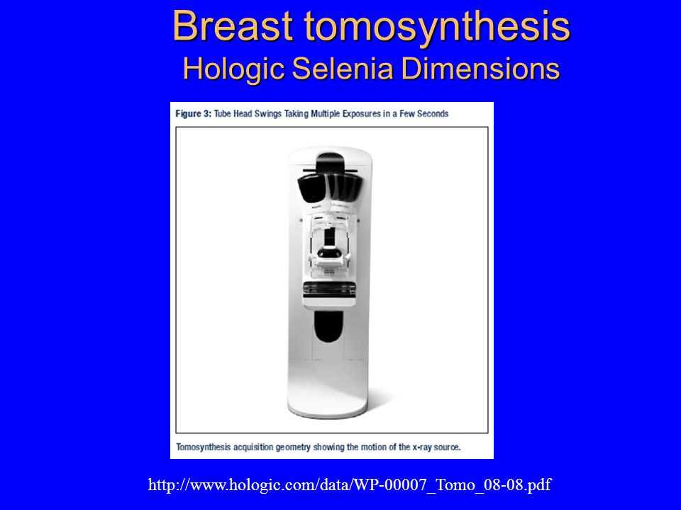
49
Breast tomosynthesis Hologic Selenia Dimensions
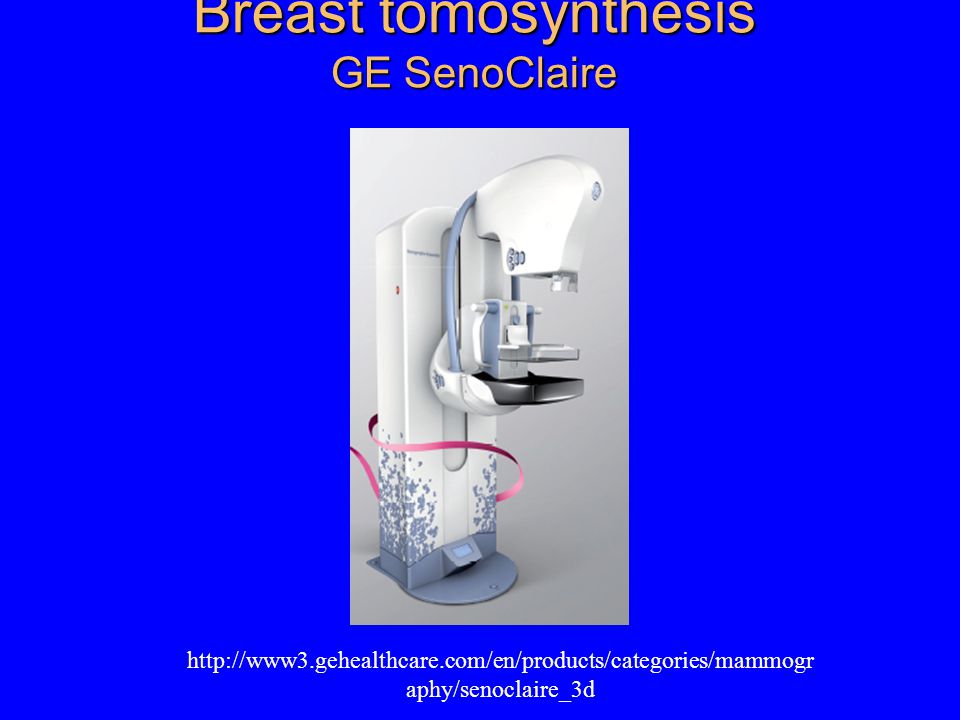
50
Breast tomosynthesis GE SenoClaire
51
Cone Beam Breast CT University of Rochester 300 views 10 seconds
University of Rochester 300 views 10 seconds

52
Breast tomosynthesis ©

53
Breast tomosynthesis

54
Breast tomosynthesis

55
DQE in Breast Tomosynthesis
Mean glandular dose (MGD) for tomosynthesis is expected to be the same as for projection mammography (< 300 mRad) Since breast tomosynthesis requires several exposures (e.g.15), low exposure DQE performance of digital detectors used in breast tomosynthesis may be very important A grid is not used in breast tomosynthesis, which reduces dose (x2 – x3)
 for tomosynthesis is expected to be the same as for projection mammography (< 300 mRad) Since breast tomosynthesis requires several exposures (e.g.15), low exposure DQE performance of digital detectors used in breast tomosynthesis may be very important. A grid is not used in breast tomosynthesis, which reduces dose (x2 – x3)")
56
Characteristics: Hologic DBT Breast Tomo
2D: one conventional FFDM image 3D Tomo: 15 views over 15 degrees that are used to reconstruct 1mm tomographic slices Combo: acquisition of both 2D and 3D tomo (still < 3 mGy) Can acquire 3D tomo in CC, MLO or any arbitrary angle
 Can acquire 3D tomo in CC, MLO or any arbitrary angle.")
57
Characteristics: Hologic DBT Breast Tomo
Data acquisition (tomo) 15 discrete views (exposures) Limited arc (15 degrees) 4 sec SID 70 cm Detector Stationary Similar to Hologic Selenia Anode Tungsten
 15 discrete views (exposures) Limited arc (15 degrees) 4 sec. SID. 70 cm. Detector. Stationary. Similar to Hologic Selenia. Anode. Tungsten.")
58
Characteristics: Hologic DBT Breast Tomo
Filters Rh: for 2D only Ag: for 2D only Al: for 3D tomo only Density control None No grid during tomo No MAGnification in tomo

59
Characteristics: Hologic DBT Breast Tomo
System resolution > 3 lp/mm (45 degrees) Tomo phantom criteria 4 fibers 3 speck groups 3 masses Can scroll up/down through 3D stack in assessing phantom scores
 Tomo phantom criteria. 4 fibers. 3 speck groups. 3 masses. Can scroll up/down through 3D stack in assessing phantom scores.")
60
Characteristics: Hologic DBT Breast Tomo
Pixel binning In 3D tomo mode, pixels are “binned” into groups of 2x2 pixels (140 micron pitch) 3D tomo collimation 18 x 29 cm exclusively Reconstruction 1 mm thick Number of tomo images: (compressed breast thickness/ 1mm => 40 – 80) Interpretation 1mm tomographic slices 15 individual projection views (good for motion detection)
 3D tomo collimation. 18 x 29 cm exclusively. Reconstruction. 1 mm thick. Number of tomo images: (compressed breast thickness/ 1mm => 40 – 80) Interpretation. 1mm tomographic slices. 15 individual projection views (good for motion detection)")
61
Characteristics: Hologic DBT Breast Tomo
Auto AEC positioning Based on intensity of 2 cells chosen from an array of 70 cells (5 x 14 with each cell occupying 1 sq.cm.)
")
62
Hologic DBT MGD 2D: 1.2 mGy 3D Tomo: 1.45 mGy Combo*: 2.65 mGy
*Combo: 2D and 3D tomo of the same breast view (e.g. MLO)
")
63
Characteristics: GE DBT Breast Tomo
3D Tomo: 9 views Step and shoot (versus continuous motion) No detector binning Tomo grid is used Iterative reconstruction (versus filtered backprojection) 3D dose same as 2D dose
 No detector binning. Tomo grid is used. Iterative reconstruction (versus filtered backprojection) 3D dose same as 2D dose.")
64
Characteristics: GE DBT Breast Tomo
V-Preview 3: a 2D image generated from the raw DBT projection data that helps the user get an overview of the entire stack, before examining the DBT planes

65
References ©NCRP 2006 ©1994 Williams & Wilkins ©1993 RSNA ©1992 RSNA
NCRP Report 149, “A Guide to Mammography and Other Breast Imaging Procedures” National Council on Radiation Protection and Measurements, 2004 ©1994 Williams & Wilkins Bushberg, JT, Seibert, JA, Leidholdt, EM Jr., Boone, JM, ”The Essential Physics of Medical Imaging” Williams & Wilkins, Baltimore, Maryland, 1994 ©1993 RSNA Haus, AG, Yaffe, MJ, Eds., “Syllabus: A Categorical Course in Physics Technical Aspects of Breast Imaging”, 2nd Edition, RSNA, 1993 ©1992 RSNA Haus, AG, Yaffe, MJ, Eds., “Syllabus: A Categorical Course in Physics Technical Aspects of Breast Imaging”, RSNA, 1992 ©1987 IOP Publishing Johns, PC, Yaffe, MJ, “X-Ray characterisation of normal and neoplastic breast tissues”, Phys Med Biol, 1987, 32,

Similar presentations


>")


: Nal scintillator/photodiode.>")


