Download presentation
Presentation is loading. Please wait.

1
Huai-Yuan Michael Tseng EE C235

2
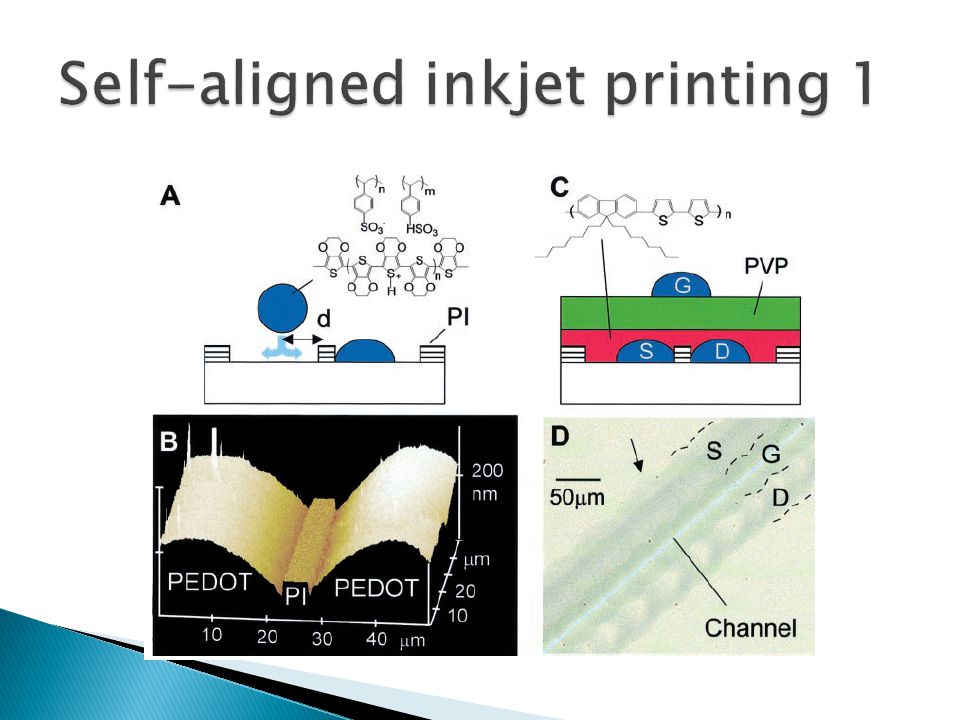
Inorganic semiconductor nanowire field effect transistors (NW-FETs) Low cost printing process ◦ Large area, flexible electronics ◦ But required sub-10um resolution ◦ Difficult to form ohmic contact when print Si NW Self-aligned inkjet printing technique Printing of metal oxide NW (ZnO)
 Low cost printing process ◦ Large area, flexible electronics ◦ But required sub-10um resolution ◦ Difficult to form ohmic contact when print Si NW Self-aligned inkjet printing technique Printing of metal oxide NW (ZnO)")
5
cyclohexylbenzene(CHB )
")
6
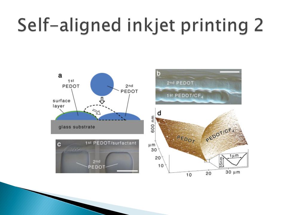
Au lift-off SAM treatment on Au Au nanoparticles printed, de-wet ZnO NW ◦ Chemical vapor deposition on a-plane sapphire substrate ◦ dispersed in IPA/ethylene glycol then inkjet printed Spin-cast PMMA Print PEDOT:PSS SAM used = 1H, 1H, 2H,2H-perflourodecanethiol PMMA = polymethyl methacrylate PEDOT:PSS = poly3,4-ethylenedioxithiophene doped with poly-styrene sulfonate

7
L=500nm Improved by heating Without ZnO With ZnO

8
All solution process ZnO NW FETs were demonstrated, however Performance limited by contact resistance as can be proved by a longer channel length device (2um) Could be improved by using lower work function metal nanoparticle or SAM treatment on Au
 Could be improved by using lower work function metal nanoparticle or SAM treatment on Au")
Similar presentations

>")

>")


 have displayed exceptional electrical properties superior to the traditional MOSFET. Most of these.>")


 and Insulated gate FETs (IGFET) There are many types of IGFET. Most common.>")


>")


