Download presentation
Presentation is loading. Please wait.

1
Carbon Nanotube Field-Effect Transistors: An Evaluation D.L. Pulfrey, L.C. Castro, D.L. John Department of Electrical and Computer Engineering University of British Columbia Vancouver, B.C. V6T1Z4, Canada pulfrey@ece.ubc.ca

2
S.Iijima, Nature 354 (1991) 56 Single-wall and multi-wall NANOTUBES Compare: flaxen hair - 20,000 nm
 56 Single-wall and multi-wall NANOTUBES Compare: flaxen hair - 20,000 nm")
3
J.Kong et al., Nature, 395, 878, 1998 CNT formation by catalytic CVD 5 m islands in PMMA patterned by EBL LPD of Fe/Mo/Al catalyst Lift-off PMMA CVD from methane at 1000C 2000nm No field Growth in field (1V/micron) A. Ural et al., Appl. Phys. Lett., 81, 3464, 2002

4
Single-Walled Carbon Nanotube 2p orbital, 1e - ( -bonds) Hybridized carbon atom graphene monolayer carbon nanotube
 Hybridized carbon atom graphene monolayer carbon nanotube")
5
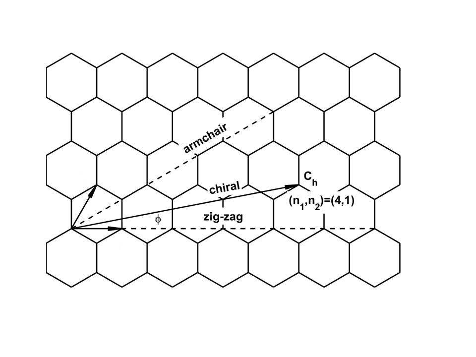
Chiral tube (5,2) Tube Structure (n,m): VECTOR NOTATION FOR NANOTUBES Adapted from Richard Martel
 Tube Structure (n,m): VECTOR NOTATION FOR NANOTUBES Adapted from Richard Martel")
6
E-E F (eV) vs. k || (1/nm) (5,0) semiconducting(5,5) metallic E g /2
 vs. k || (1/nm) (5,0) semiconducting(5,5) metallic E g /2")
7
Doping Substitutional unlikely Adsorbed possible e.g., K, O Interior possible Tubes are naturally intrinsic

8
Phonons Acoustic phonons (twistons) mfp 300 nm Ballistic transport possible Optical phonons mfp 15 nm
 mfp 300 nm Ballistic transport possible Optical phonons mfp 15 nm")
9
Fabricated Carbon Nanotube FETs Few prototypes –[Tans98]: 1 st published device –[Wind02]: Top-gated CNFET –[Rosenblatt02]: Electrolyte-gated Nanotube
![Fabricated Carbon Nanotube FETs Few prototypes –[Tans98]: 1 st published device –[Wind02]: Top-gated CNFET –[Rosenblatt02]: Electrolyte-gated Nanotube](http://images.slideplayer.com/15/4793698/slides/slide_9.jpg "Fabricated Carbon Nanotube FETs Few prototypes –[Tans98]: 1 st published device –[Wind02]: Top-gated CNFET –[Rosenblatt02]: Electrolyte-gated Nanotube")
10
CLOSED COAXIAL NANOTUBE FET STRUCTURE chirality: (16,0) radius: 0.62 nm bandgap: 0.63 eV length: 15 - 100 nm oxide thickness: (R G -R T ): 2 - 6 nm
 radius: 0.62 nm bandgap: 0.63 eV length: nm oxide thickness: (R G -R T ): nm")
11
kxkx kxkx kzkz E METAL (many modes) CNT (few modes) Doubly degenerate lowest mode MODE CONSTRICTION and TRANSMISSION T
 CNT (few modes) Doubly degenerate lowest mode MODE CONSTRICTION and TRANSMISSION T")
12
gate insulator nanotube C ins CQCQ Quantum Capacitance Limit EbEb source

13
Quantum Capacitance and Sub-threshold Slope High k dielectrics: zirconia - 25 water - 80 70 mV/decade ! - Javey et al., Nature Materials, 1, 241, 2002

14
AMBIPOLAR CONDUCTION Experimental data: M. Radosavljevic et al., arXiv: cond-mat/0305570 v1 Vds= - 0.4V Vgs= -0.15 +0.05 +0.30

15
Minimize the OFF Current G = 4.2 eV Increasing S,D 3.9, 4.2, 4.5 eV S,D = 3.9 eV Increasing G 3.0, 4.37 eV ON/OFF 10 3

16
General non-equilibrium case E f(E) E FS 0.5 E f(E) E FD 0.5 g(E) E 1D DOS Non-equilib f(E) Q(z,E)=qf(E)g(E) Solve Poisson iteratively
 E FS 0.5 E f(E) E FD 0.5 g(E) E 1D DOS Non-equilib f(E) Q(z,E)=qf(E)g(E) Solve Poisson iteratively")
17
CURRENT in 1-D SYSTEMS

18
Quantized Conductance In the low-temperature limit: Interfacial G: even when transport is ballistic in CNT 155 S for M=2

19
Measured Conductance A. Javey et al., Nature, 424, 654, 2003 No tunneling barriers Low R contacts (Pd) G 0.4 G max at 280K !!
 G 0.4 G max at 280K !!.")
20
Drain Saturation Current If T=1 Get BJT behaviour! V GS EbEb EFEF Zero-height Schottky barrier

21
Present world record Javey et al., Nature, 424, 654, 2003 ON Current: Measured and Possible S,D = 3.9eV G = 4.37eV C Q limit 80% of QC limit!

22
Predicted Drain Current -ve 0 +ve Vgs=Vds=0.4V 70mA/ m !!

23
Transconductance Low V DS : modulate for G High V DS : modulate V GS for g m

24
Transconductance: Measured and Possible Highest measured: Rosenblatt et al. Nano. Lett., 2, 869, 2002 C Q limit S,D = 3.9eV G = 4.37eV 80% of QC limit!

25
CNFET Logic A.Javey et al., Nature Materials, 1, 241, 2002 Gain=60 1 st OR-gate 0,0

26
Williams, Veenhuizen, de la Torre, Eritja and Dekker Nature, 420, 761, 2002. CNTs Functionalized with DNA Recognition-based assembly

27
Self-assembly of DNA-templated CNFETs K.Keren et al., Technion.

29
CONCLUSIONS Schottky barriers play a crucial role in determining the drain current. Negative barrier devices enable: control of ambipolarity, high ON/OFF ratios, near ultimate-limit S, G, I D, g m. CNFETs can be self-assembled via biological recognition. CNs have excellent thermal and mechanical properties. CNFETs deserve serious study as molecular transistors.

30
Extra Slides

31
Nanoscale Bandgap tunability Metals and semiconductors Ballistic transport Strong covalent bonding: -- strength and stability of graphite -- reduced electromigration (high current operation) -- no surface states (less scattering, compatibility with many insulators) High thermal conductivity -- almost as high as diamond (dense circuits) Let’s make transistors! Compelling Properties of Carbon Nanotubes

32
From: Dresselhaus, Dresselhaus & Eklund. 1996 Science of Fullerenes and Carbon Nanotubes. San Diego, Academic Press. Adapted from Richard Martel. Armchair Zig-Zag Chiral CHIRAL NANOTUBES

34
Carbon Nanotube Properties Graphene sheet 2D E(k //,k ) –Quantization of transverse wavevectors k (along tube circumference) Nanotube 1D E(k // ) Nanotube 1D density-of-states derived from [ E(k // )/ k] -1 Get E(k // ) vs. k(k //,k ) from Tight-Binding Approximation
![Carbon Nanotube Properties Graphene sheet 2D E(k //,k ) –Quantization of transverse wavevectors k (along tube circumference) Nanotube 1D E(k // ) Nanotube 1D density-of-states derived from [ E(k // )/ k] -1 Get E(k // ) vs.](http://images.slideplayer.com/15/4793698/slides/slide_34.jpg "k(k //,k ) from Tight-Binding Approximation.")
35
Density of States k || or k z

36
Tight Binding David John, UBC Wolfe et al., “Physical Properties of Semiconductors”

37
Density of States (5,0) tube David John E(eV) vs. k || (1/nm) E(eV) vs. DOS (100/eV/nm)
 tube David John E(eV) vs. k || (1/nm) E(eV) vs. DOS (100/eV/nm)")
38
Tuning the Bandgap T. Odom et al., Nature, 391, 62, 1998 E g 7 nm “zero bandgap” semiconductor

39
nanotube oxide gate Planar Coaxial The Ideal Structure

40
J.Kong et al., Nature, 395, 878, 1998 CNT formation by catalytic CVD 5 m islands in PMMA patterned by EBL LPD of Fe/Mo/Al catalyst Lift-off PMMA CVD from methane at 1000C 1000nm 300nm 2000nm

41
CNT formation by E-field assisted CVD A. Ural et al., Appl. Phys. Lett., 81, 3464, 2002 V applied between Mo electrodes. CVD from catalytic islands. No field 10V applied

42
Bottom-gated Nanotube FETs A. Javey et al., Nature, 424, 654, 2003 Note very high I D 10mA/ m Nanotube 1 st CNFET S. Tans et al., Nature, 393, 49, 1998

43
Phenomenological treatment of metal/nanotube contacts Evidence of work function-dependence of I-V : A. Javey et al., Nature, 424, 654, 2003 Zero hole barrier

44
Schrödinger-Poisson Model Need full QM treatment to compute: -- Q(z) within positive barrier regions -- Q in evanescent states (MIGS) -- S D tunneling -- resonance, coherence
 within positive barrier regions -- Q in evanescent states (MIGS) -- S D tunneling -- resonance, coherence")
45
Schrödinger-Poisson Model L.C. Castro, D.L. John SDCNT Unbounded plane waves

46
Increasing the Drain Current Vgs=Vds=0.4V 70mA/ m !!

47
Array of vertically grown CNFETs W.B. Choi et al., Appl. Phys. Lett., 79, 3696, 2001. 2x10 11 CNTs/cm 2 !!

Similar presentations


>")

 have displayed exceptional electrical properties superior to the traditional MOSFET. Most of these.>")


 Alexandra Ford NSE 203/EE 235 Class Presentation March 5, 2007.>")


